
Read and download the CBSE Class 12 Physics Semiconductor Devices Worksheet Set 02 in PDF format. We have provided exhaustive and printable Class 12 Physics worksheets for Chapter 14 Semiconductor Electronics Materials Devices and Simple Circuits, designed by expert teachers. These resources align with the 2026-27 syllabus and examination patterns issued by NCERT, CBSE, and KVS, helping students master all important chapter topics.
Chapter-wise Worksheet for Class 12 Physics Chapter 14 Semiconductor Electronics Materials Devices and Simple Circuits
Students of Class 12 should use this Physics practice paper to check their understanding of Chapter 14 Semiconductor Electronics Materials Devices and Simple Circuits as it includes essential problems and detailed solutions. Regular self-testing with these will help you achieve higher marks in your school tests and final examinations.
Class 12 Physics Chapter 14 Semiconductor Electronics Materials Devices and Simple Circuits Worksheet with Answers
Important Questions for NCERT Class 12 Physics Semiconductor Devices
Question. An amplifier has a voltage gain Av = 1000. The voltage gain in dB is:
(a) 30 dB
(b) 60 dB
(c) 3 dB
(d) 20 dB
Answer: A
Question. If the highest modulating frequency of the wave is 5 kHz, the number of stations that can be accomdated in a 150 kHz bandwidth are
(a) 15
(b) 10
(c) 5
(d) none of these
Answer: A
Question. Number of atom per unit cell in B.C.C.
(a) 9
(b) 4
(c) 2
(d) 1
Answer: C
Question. The cations and anions are arranged in alternate form in
(a) metallic crystal
(b) ionic crystal
(c) covalent crystal
(d) semi-conductor crystal.
Answer: B
Question. Distance between body centred atom and a corner atom in sodium (a = 4.225 Å) is
(a) 2.99 Å
(b) 2.54 Å
(c) 3.66 Å
(d) 3.17 Å.
Answer: C
Question. Diamond is very hard because
(a) it is covalent solid
(b) it has large cohesive energy
(c) high melting point
(d) insoluble in all solvents.
Answer: B
Question. Which one of the following is the weakest kind of the bonding in solids?
(a) ionic
(b) metallic
(c) van der Waals
(d) covalent
Answer: C
Question. In p-type semiconductor major current carriers are :
(a) negative ions
(b) holes
(c) electrons
(d) all of these
Answer: B
Question. In a diode, when there is a saturation current, the plate resistance will be
(a) data insufficient
(b) zero
(c) some finite quantity
(d) infinite quantity
Answer: D
Question. When the two semiconductors p- and n-type are brought into contact they form a p-n junction, which acts like a/an :
(a) rectifier
(b) amplifier
(c) conductor
(d) oscillator
Answer: A
Question. The transfer ratio b of a transistor is 50. The input resistance of the transistor when used in the common emitter configuration is 1kW. The peak value of the collector A.C. current for an A.C. input voltage of 0.01 V, is
(a) 500 μA
(b) 0.25 μA
(c) 0.01 μA
(d) 100 μA
Answer: A
Question. When n-p-n transistor is used as an amplifier, then
(a) electrons move from base to collector
(b) holes move from emitter to base
(c) electrons move from collector to base
(d) holes move from base to emitter
Answer: A
Question. Boolean algebra is essentially based on:
(a) Numbers
(b) Symbol
(c) Logic
(d) Truth
Answer: C
Question. A triode valve has an amplification factor of 20 and its plate is given a potential of 300 V. The grid voltage to reduce the plate current to zero, is
(a) 25 V
(b) 15 V
(c) 12 V
(d) 10 V
Answer: B
Question. Diode is used as a/an
(a) modulator
(b) rectifier
(c) oscillator
(d) amplifier
Answer: B
Question. In n-type semiconductor, majority charge carriers are
(a) electrons
(b) neutrons
(c) holes
(d) protons
Answer: A
Question. In a common emitter (CE) amplifier having a voltage gain G, the transistor used has transconductance 0.03 mho and current gain 25. If the above transistor is replaced with another one with transconductance 0.02 mho and current gain 20, the voltage gain will be
(a) 1.5 G
(b) 1/3 G
(c) 5/4 G
(d) 2/3 G
Answer: D
Question. An oscillator is nothing but an amplifier with
(a) positive feedback
(b) large gain
(c) no feedback
(d) negative feedback
Answer: A
Question. The conductivity of a semiconductor increases with increase in temperature because
(a) number density of free current carries increases
(b) relaxation time increases
(c) both number density of carries and relaxation time increase
(d) number density of carries increases, relaxation time decreases but effect of decrease in relaxation time is much less than increase in number density
Answer: D
Question. Barrier potential of a P-N junction diode does not depend on
(a) doping density
(b) diode design
(c) temperature
(d) forward bias
Answer: B
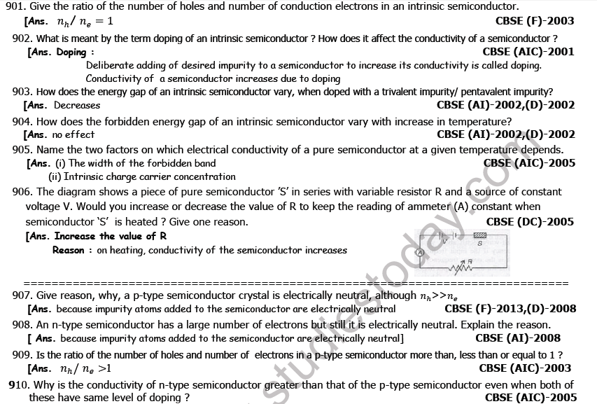
Question. The real time variation of input signals A and B are as shown below. If the inputs are fed into NAND gate, then select the output signal from the following. 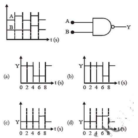
Answer: B
Question. Reverse bias applied to a junction diode
(a) increases the minority carrier current
(b) lowers the potential barrier
(c) raises the potential barrier
(d) increases the majority carrier current
Answer: C
Question. In semiconductors at a room temperature
(a) the conduction band is completely empty
(b) the valence band is partially empty and the conduction band is partially filled
(c) the valence band is completely filled and the conduction band is partially filled
(d) the valence band is completely filled
Answer: C
Question. One serious drawback of semi-conductor devices is
(a) they do not last for long time.
(b) they are costly
(c) they cannot be used with high voltage.
(d) they pollute the environment.
Answer: C
Question. The peak voltage in the output of a half-wave diode rectifier fed with a sinusoidal signal without filter is 10V. The d.c. component of the output voltage is
(a) 20/π V
(b) 10/√2 V
(c) 10/π V
(d) 10V
Answer: C
Question. In a p-n junction photo cell, the value of the photoelectromotive force produced by monochromatic light is proportional to
(a) the voltage applied at the p-n junction
(b) the barrier voltage at the p-n junction
(c) the intensity of the light falling on the cell
(d) the frequency of the light falling on the cell
Answer: C
Question. Of the diodes shown in the following diagrams, which one is reverse biased ? 
Answer: D
Question. Choose the only false statement from the following.
(a) In conductors the valence and conduction bands may overlap.
(b) Substances with energy gap of the order of 10 eV are insulators.
(c) The resistivity of a semiconductor increases with increase in temperature.
(d) The conductivity of a semiconductor increases with increase in temperature.
Answer: C
Question. Which one of the following statement is false ?
(a) Pure Si doped with trivalent impurities gives a p-type semiconductor
(b) Majority carriers in a n-type semiconductor are holes
(c) Minority carriers in a p-type semiconductor are electrons
(d) The resistance of intrinsic semiconductor decreases with increase of temperature
Answer: B
Question. The figure shows a logic circuit with two inputs A and B and the output C. The voltage wave forms across A, B and C are as given. The logic gate circuit is: 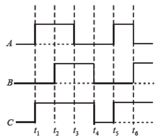
(a) OR gate
(b) NOR gate
(c) AND gate
(d) NAND gate
Answer: A
Question. In a P -N junction
(a) the potential of P & N sides becomes higher alternately
(b) the P side is at higher electrical potential than N side.
(c) the N side is at higher electric potential than P side.
(d) both P & N sides are at same potential.
Answer: B
Question. The time variations of signals are given as in A, B and C. Point out the true statement from the following :
(a) A, B and C are analogue signals
(b) A and B are analogue, but C is digital signal
(c) A and C are digital, but B is analogue signal
(d) A and C are analogue, but B is digital signal
Answer: D
Question. A common emitter amplifier has a voltage gain of 50, an input impedance of 100Ω and an output impedance of 200Ω. The power gain of the amplifier is
(a) 500
(b) 1000
(c) 1250
(d) 50
Answer: C
Question. A npn transistor is connected in common emitter configuration in a given amplifier. A load resistance of 800 Ω is connected in the collector circuit and the voltage drop across it is 0.8 V. If the current amplification factor is 0.96 and the input resistance of the circuit is 192Ω, the voltage gain and the power gain of the amplifier will respectively be:
(a) 4, 3.84
(b) 3.69, 3.84
(c) 4, 4
(d) 4, 3.69
Answer: A
Question. In common emitter amplifier, the current gain is 62. The collector resistance and input resistance are 5 kΩ an 500Ω respectively. If the input voltage is 0.01 V, the output voltage is
(a) 0.62 V
(b) 6.2 V
(c) 62 V
(d) 620 V
Answer: B
Question. The output(X) of the logic circuit shown in figure will be 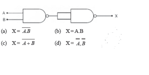
Answer: B
Please click the link below to download pdf file of Class 12 Physics Semiconductor Electronic Devices Boards Questions
Free study material for Physics
CBSE Physics Class 12 Chapter 14 Semiconductor Electronics Materials Devices and Simple Circuits Worksheet
Students can use the practice questions and answers provided above for Chapter 14 Semiconductor Electronics Materials Devices and Simple Circuits to prepare for their upcoming school tests. This resource is designed by expert teachers as per the latest 2026 syllabus released by CBSE for Class 12. We suggest that Class 12 students solve these questions daily for a strong foundation in Physics.
Chapter 14 Semiconductor Electronics Materials Devices and Simple Circuits Solutions & NCERT Alignment
Our expert teachers have referred to the latest NCERT book for Class 12 Physics to create these exercises. After solving the questions you should compare your answers with our detailed solutions as they have been designed by expert teachers. You will understand the correct way to write answers for the CBSE exams. You can also see above MCQ questions for Physics to cover every important topic in the chapter.
Class 12 Exam Preparation Strategy
Regular practice of this Class 12 Physics study material helps you to be familiar with the most regularly asked exam topics. If you find any topic in Chapter 14 Semiconductor Electronics Materials Devices and Simple Circuits difficult then you can refer to our NCERT solutions for Class 12 Physics. All revision sheets and printable assignments on studiestoday.com are free and updated to help students get better scores in their school examinations.
FAQs
You can download the latest chapter-wise printable worksheets for Class 12 Physics Chapter 14 Semiconductor Electronics Materials Devices and Simple Circuits for free from StudiesToday.com. These have been made as per the latest CBSE curriculum for this academic year.
Yes, Class 12 Physics worksheets for Chapter 14 Semiconductor Electronics Materials Devices and Simple Circuits focus on activity-based learning and also competency-style questions. This helps students to apply theoretical knowledge to practical scenarios.
Yes, we have provided solved worksheets for Class 12 Physics Chapter 14 Semiconductor Electronics Materials Devices and Simple Circuits to help students verify their answers instantly.
Yes, our Class 12 Physics test sheets are mobile-friendly PDFs and can be printed by teachers for classroom.
For Chapter 14 Semiconductor Electronics Materials Devices and Simple Circuits, regular practice with our worksheets will improve question-handling speed and help students understand all technical terms and diagrams.