

Chapter-wise Worksheets for Class 12 Physics: 2 Mark Question Bank
Explore structured practice materials through the CBSE Class 12 Physics 2 Mark Question Bank Worksheet. Tailored for Class 12 learners, utilizing these Physics worksheets ensures thorough preparation and strengthens problem-solving accuracy before final school evaluations.
Practice Class 12 Physics Worksheets: 2 Mark Question Bank
View or download the dedicated CBSE Class 12 Physics 2 Mark Question Bank Worksheet resource below. Engaging with these practice papers under focused study conditions ensures continuous academic progress and mastery of the 2026-27 curriculum for 2 Mark Question Bank.
CBSE Class 12 Physics 2 mark Question Bank. Students can download these worksheets and practice them. This will help them to get better marks in examinations. Also refer to other worksheets for the same chapter and other subjects too. Use them for better understanding of the subjects.
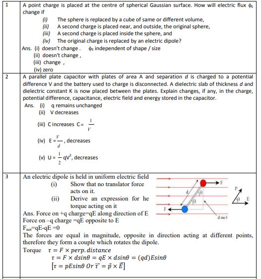
2 Marks Questions
Question 1. A point charge is placed at the centre of spherical Gaussian surface. How will electric flux E change if
(i) The sphere is replaced by a cube of same or different volume,
(ii) A second charge is placed near, and outside, the original sphere,
(iii) A second charge is placed inside the sphere, and
(iv) The original charge is replaced by an electric dipole?
Answer:
(i) **Replacing the sphere with a cube:** The electric flux remains unchanged. According to Gauss's law, the electric flux through a closed surface depends only on the charge enclosed inside it and is completely independent of the shape or size of the surface.
(ii) **Placing a second charge outside:** The electric flux remains unchanged. A charge located outside the Gaussian surface does not contribute to the net flux passing through that surface.
(iii) **Placing a second charge inside:** The electric flux changes. The net enclosed charge increases or decreases depending on the sign of the second charge, which directly alters the net electric flux.
(iv) **Replacing with an electric dipole:** The electric flux becomes zero. An electric dipole consists of equal and opposite charges (\( +q \) and \( -q \)), so the net charge enclosed within the Gaussian surface is zero, resulting in zero net flux.
In simple words: The total electric flux through any closed boundary only depends on the net charge inside it. Changing the shape of the surface or placing charges outside does not affect the flux, but putting an electric dipole inside makes the net charge zero, resulting in zero flux.
Exam Tip: State Gauss's law formula \( \Phi_E = \frac{q}{\varepsilon_0} \) explicitly to show that flux is solely determined by the enclosed net charge and nothing else.
Question 2. A parallel plate capacitor with plates of area A and separation d is charged to a potential difference V and the battery used to charge is disconnected. A dielectric slab of thickness d and dielectric constant K is now placed between the plates. Explain changes, if any, in the charge, potential difference, capacitance, electric field and energy stored in the capacitor.
Answer: When the battery is disconnected and a dielectric slab of dielectric constant \( K \) is inserted to fill the entire gap, the physical quantities change as follows:
(i) **Charge (\( q \)):** Remains completely unchanged (\( q' = q \)) because the capacitor is isolated from the battery, so there is no path for the charge to leave or enter the plates.
(ii) **Potential Difference (\( V \)):** Decreases to \( V' = \frac{V}{K} \) because the dielectric material sets up an opposing internal electric field through polarization, which reduces the potential difference across the plates.
(iii) **Capacitance (\( C \)):** Increases by a factor of \( K \) (\( C' = K \cdot C \)). Since capacitance is \( C = \frac{q}{V} \), the decrease in potential difference with a constant charge results in a proportional increase in capacitance.
(iv) **Electric Field (\( E \)):** Decreases to \( E' = \frac{E}{K} \). The electric field is related to potential by \( E = \frac{V}{d} \); since the plate spacing \( d \) is constant and \( V \) decreases, the electric field decreases accordingly.
(v) **Energy Stored (\( U \)):** Decreases to \( U' = \frac{U}{K} \). The electrostatic energy stored is \( U = \frac{q^2}{2C} \). Since \( q \) remains constant and the capacitance \( C \) increases by a factor of \( K \), the stored energy drops to \( \frac{1}{K} \) of its original value.
In simple words: Once the battery is disconnected, the charge on the plates is locked in place. Adding a dielectric material reduces the electric field and voltage between the plates by a factor of K, which boosts the capacitance and lowers the stored energy.
Exam Tip: Clearly state that the charge remains constant whenever the battery is disconnected, while the potential difference remains constant if the battery remains connected during the process.
Question 3. An electric dipole is held in uniform electric field
(i) Show that no translator force acts on it.
(ii) Derive an expression for he torque acting on it
Answer:
(i) **No Translatory Force:**
Consider an electric dipole consisting of two charges \( +q \) and \( -q \) separated by a distance \( d \) in a uniform electric field \( \vec{E} \).
- The force acting on the charge \( +q \) is \( \vec{F}_1 = q\vec{E} \), which acts in the direction of the electric field.
- The force acting on the charge \( -q \) is \( \vec{F}_2 = -q\vec{E} \), which acts in the direction opposite to the electric field.
The net translational force acting on the dipole is: \[ \vec{F}_{\text{net}} = \vec{F}_1 + \vec{F}_2 = q\vec{E} - q\vec{E} = 0 \] Hence, there is no net translational force on the dipole in a uniform electric field.
(ii) **Expression for Torque:**
Although the net force is zero, the two equal and opposite forces act at different points along different lines of action. This set of forces forms a couple, which produces a torque that tends to align the dipole with the field.
The magnitude of the torque (\( \tau \)) is given by: \[ \tau = \text{Force} \times \text{Perpendicular distance between the two forces} \] From the geometry of the dipole in the field, the perpendicular distance between the lines of action of the forces is \( d \sin \theta \), where \( \theta \) is the angle between the dipole moment \( \vec{p} \) and the electric field \( \vec{E} \). \[ \tau = (qE) \times (d \sin \theta) \] Since the electric dipole moment is \( p = q \cdot d \), we can write: \[ \tau = p E \sin \theta \] In vector notation, the torque is: \[ \vec{\tau} = \vec{p} \times \vec{E} \]
In simple words: Inside a uniform electric field, the positive and negative charges of a dipole experience equal but opposite forces, which cancel out so the dipole doesn't move sideways. However, because these forces pull at different points, they twist the dipole to align it with the field.
Exam Tip: Be sure to write both the scalar expression \( \tau = p E \sin \theta \) and the vector cross product \( \vec{\tau} = \vec{p} \times \vec{E} \), noting that the direction of torque is perpendicular to the plane containing both \( \vec{p} \) and \( \vec{E} \).
Question 4. How does the resistivity of (i) a conductor and (ii) a semiconductor vary with temperature? Give reasons.
Answer: The electrical resistivity \( \rho \) of a material is given by the relation: \[ \rho = \frac{m}{n e^2 \tau} \] where \( m \) is the mass of an electron, \( e \) is the charge of an electron, \( n \) is the number density of free electrons, and \( \tau \) is the relaxation time.
(i) **For a Conductor:**
In metallic conductors, the number density of free electrons \( n \) is extremely large and remains virtually independent of temperature variations. However, as the temperature rises, the thermal agitation of lattice ions increases, causing more frequent collisions with electrons. Consequently, the relaxation time \( \tau \) decreases. Since \( \rho \propto \frac{1}{\tau} \), the resistivity of a conductor increases as the temperature increases.
(ii) **For a Semiconductor:**
In semiconductors, raising the temperature provides enough thermal energy to break covalent bonds, which significantly increases the free charge carrier density \( n \). Although the relaxation time \( \tau \) decreases slightly due to increased thermal collisions, the exponential increase in the carrier density \( n \) dominates over the small decrease in \( \tau \). Since \( \rho \propto \frac{1}{n \tau} \), the net resistivity of a semiconductor decreases exponentially as temperature rises.
In simple words: (i) Heating a metal makes its atoms vibrate wildly, blocking the path of electrons (reducing relaxation time), which increases its resistance. (ii) In semiconductors, heat frees up many more charge carriers, which vastly improves its ability to conduct, thereby lowering its resistivity.
Exam Tip: Use the formula \( \rho = \frac{m}{n e^2 \tau} \) as the starting point of your explanation. Clearly state which parameter (\( \tau \) for metals, \( n \) for semiconductors) dominates the temperature response.
Page 2
Question 5. Define the term resistivity and write its SI unit. Derive the expression for the resistivity of a conductor in terms of number density of free electrons and relaxation time.
Answer: **Definition:** The resistivity of a material is defined as the resistance offered by a conductor of unit length and unit cross-sectional area. Alternatively, it is the resistance of a unit cube of the given material.
**SI Unit:** Ohm-meter (\( \Omega \cdot \text{m} \)).
**Derivation:**
The current \( I \) flowing through a conductor of length \( l \) and cross-sectional area \( A \) is given by: \[ I = n e A v_d \quad \text{--- (1)} \] where \( v_d \) is the drift velocity of free electrons, which is expressed as: \[ v_d = \frac{e E}{m} \tau \quad \text{--- (2)} \] Since the electric field \( E \) inside the conductor is \( E = \frac{V}{l} \), where \( V \) is the potential difference, we substitute \( E \) into equation (2): \[ v_d = \frac{e V}{m l} \tau \] Substituting the value of \( v_d \) into equation (1), we get: \[ I = n e A \left( \frac{e V}{m l} \tau \right) = \left( \frac{n e^2 A \tau}{m l} \right) V \] Rearranging this to find the ratio \( \frac{V}{I} \) (which is resistance \( R \)): \[ R = \frac{V}{I} = \left( \frac{m}{n e^2 \tau} \right) \frac{l}{A} \quad \text{--- (3)} \] By definition, the electrical resistance \( R \) is also expressed as: \[ R = \rho \frac{l}{A} \quad \text{--- (4)} \] Comparing equations (3) and (4), we obtain the expression for resistivity \( \rho \): \[ \rho = \frac{m}{n e^2 \tau} \]
In simple words: Resistivity is a material's natural resistance for a standard block size. By using the link between electric current, electron drift velocity, and applied voltage, we find that the resistivity depends solely on the mass and charge of the electron, the free electron density, and the relaxation time.
Exam Tip: Make sure to define every term used in the derivation (\( m, n, e, \tau, v_d \)) clearly. Examiners look for the comparison between Ohm's law and the resistance formula to award full marks.
Question 6. Two students ‘X’ and ‘Y’ perform an experiment on potentiometer separately using the circuit given. Keeping other parameters unchanged, how will the position of the null point be affected it (i) ‘X’ increases the value of resistance R in the set-up by keeping the key K1 closed and the key K2 open? (ii) ‘Y’ decreases the value of resistance S in the set-up, while the key K2 remain open and the key K1 closed? Justify.
Answer:
(i) **When resistance \( R \) is increased:**
When the external resistance \( R \) in the primary circuit is increased, the total current flowing through the potentiometer wire AB decreases. This reduction in current causes a decrease in the potential drop per unit length of the wire, which is called the potential gradient (\( k \)). Since the balancing length is inversely proportional to the potential gradient (\( l \propto \frac{1}{k} \)), a larger length of the wire is required to balance the same electromotive force. Consequently, the null point shifts towards the end **B**.
(ii) **When resistance \( S \) is decreased:**
Since the key \( K_2 \) remains open, no current flows through the resistor \( S \) in the secondary circuit. The cell in the secondary circuit remains in an open circuit state, and we are measuring its true electromotive force (\( E_1 \)). Since the primary current and potential gradient across the wire AB remain completely unchanged, changing the value of \( S \) has no effect. Thus, the position of the null point remains **unchanged**.
In simple words: (i) Increasing R cuts down the current in the main wire, making the voltage drop slower along its length, so the detector has to slide further towards B to find the balance. (ii) Since the second switch is off, no current flows through S anyway, so changing its value has zero impact on the balance point.
Exam Tip: Remember that changing secondary circuit components has absolutely zero effect on the null point position if the key \( K_2 \) remains open, as no current can flow through them.
Question 7. Define the term magnetic dipole moment of a current loop. Write the expression for the magnetic moment when an electron revolves at a speed ‘v’, around an orbit of radius ‘ r’ in hydrogen atom.
Answer:
**Definition:** The magnetic dipole moment \( M \) of a current-carrying loop is defined as the product of the number of turns \( N \) in the loop, the current \( I \) flowing through the loop, and the area \( A \) enclosed by the loop. \[ M = N I A \] **Direction:** Its direction is perpendicular to the plane of the loop and can be found using the right-hand thumb rule.
**Revolving Electron in a Hydrogen Atom:**
An electron of charge \( e \) revolving around a nucleus of radius \( r \) with speed \( v \) has a time period of revolution: \[ T = \frac{2\pi r}{v} \] The equivalent electric current \( I \) associated with this motion is: \[ I = \frac{e}{T} = \frac{e v}{2\pi r} \] The area enclosed by the circular orbit of the electron is \( A = \pi r^2 \). Thus, the magnetic moment \( M \) of this revolving electron is: \[ M = I A = \left( \frac{e v}{2\pi r} \right) \left( \pi r^2 \right) = \frac{e v r}{2} \]
In simple words: The magnetic strength of a loop is simply its current multiplied by its area. When an electron circles the nucleus in a hydrogen atom, its circular motion acts like a tiny current loop, producing a magnetic moment equal to half the product of its charge, speed, and radius.
Exam Tip: Be sure to write the derivation of the revolving electron current \( I = \frac{ev}{2\pi r} \) clearly before writing the final formula \( M = \frac{evr}{2} \). Mentioning the right-hand thumb rule for direction is also key.
Page 3
Question 8. The following figure shows the variation of intensity of magnetization I versus the applied magnetic field intensity H for two magnetic materials A and B.
(1) Identify the materials A and B
(2) Draw the variation of susceptibility with temperature for B.
Answer:
(1) **Identification of Materials:**
- **Material A is Paramagnetic:** For paramagnetic materials, the intensity of magnetization \( I \) increases linearly and positively with the applied magnetic field \( H \), meaning the susceptibility \( \chi = \frac{I}{H} \) is small and positive.
- **Material B is Diamagnetic:** For diamagnetic materials, the magnetization \( I \) is induced in a direction opposite to the applied magnetic field, resulting in a negative slope, meaning the susceptibility \( \chi \) is negative.
(2) **Susceptibility vs Temperature for Diamagnetic Material (B):**
Since diamagnetism is independent of temperature, the magnetic susceptibility \( \chi \) of a diamagnetic material does not change with temperature. The graph of susceptibility \( \chi \) versus temperature \( T \) is a straight horizontal line in the negative region.
In simple words: (1) Material A gets magnetized in the same direction as the field, so it is paramagnetic. Material B gets weakly magnetized in the opposite direction, making it diamagnetic. (2) Since diamagnetism is completely unaffected by temperature, its magnetic susceptibility remains a flat horizontal line below zero.
Exam Tip: Always make sure to draw the \( \chi \) vs \( T \) graph below the temperature axis (in the negative quadrant) because the susceptibility of diamagnetic materials is negative.
Question 9. How does the self induction of a coil change when?
(1) The number of turns in a coil is decreased
(2) An iron rod is introduced into it. Justify.
Answer:
The self-inductance \( L \) of a long solenoid (coil) of length \( l \), cross-sectional area \( A \), and total number of turns \( N \) is given by: \[ L = \frac{\mu_0 \mu_r N^2 A}{l} \] where \( \mu_0 \) is the permeability of free space and \( \mu_r \) is the relative permeability of the core material.
(1) **When the number of turns is decreased:**
Since the self-inductance \( L \) is directly proportional to the square of the total number of turns (\( L \propto N^2 \)), decreasing the number of turns will cause a significant decrease in the self-inductance of the coil.
(2) **When an iron rod is introduced:**
For air, the relative permeability is \( \mu_r = 1 \). When a soft iron rod is inserted into the coil, the core material changes to iron, which is ferromagnetic and has a very high relative permeability (\( \mu_r \gg 1 \)). Consequently, the self-inductance of the coil will increase tremendously (by a factor of \( \mu_r \)).
In simple words: (1) Since inductance depends on the square of the number of wire loops, removing loops reduces the coil's magnetic strength and its self-inductance. (2) Inserting an iron rod dramatically boosts the magnetic field lines inside the coil, increasing its self-inductance.
Exam Tip: Be sure to write the formula \( L = \frac{\mu_0 \mu_r N^2 A}{l} \) to justify your answers. Explicitly state the dependency of \( L \) on both the square of the number of turns \( N^2 \) and the relative permeability \( \mu_r \).
Question 10. An inductor L of reactance XL is connected in series with a bulb B to an a.c. source as shown in the figure.
Briefly explain how does the brightness of the bulb change when
(a) Number of turns of the inductor is reduced.
(b) A capacitor of reactance Xc = XL is included in series in the same circuit.
Answer:
The impedance \( Z \) of a series \( LR \) or \( LCR \) circuit determines the current \( I \) flowing through the bulb (which acts as a resistor \( R \)): \[ I = \frac{V}{Z} \] The brightness of the bulb is directly proportional to the square of the current flowing through it (\( P = I^2 R \)).
(a) **When the number of turns of the inductor is reduced:**
Reducing the number of turns decreases the self-inductance \( L \) of the coil. Since the inductive reactance is \( X_L = \omega L \), the value of \( X_L \) also decreases. This, in turn, reduces the total impedance \( Z = \sqrt{R^2 + X_L^2} \) of the circuit. As the impedance decreases, the circuit current \( I \) increases, causing the bulb to **glow more brightly**.
(b) **When a capacitor of reactance \( X_C = X_L \) is included in series:**
The net impedance \( Z \) of the resulting \( LCR \) series circuit is given by: \[ Z = \sqrt{R^2 + (X_L - X_C)^2} \] Since \( X_C = X_L \), the reactive term becomes zero, and the impedance reduces to its minimum possible value: \[ Z = R \] This state corresponds to electrical resonance. As the impedance becomes minimum, the current in the circuit reaches its maximum value. Therefore, the brightness of the bulb becomes **maximum**.
In simple words: (a) Removing loops from the coil lowers its electrical barrier (reactance), allowing more current to flow, which makes the bulb glow brighter. (b) Adding a capacitor that perfectly cancels out the coil's barrier creates resonance. Since the total barrier drops to just the bulb's resistance, the maximum possible current flows, making the bulb shine with peak brightness.
Exam Tip: Be sure to write the formula for impedance \( Z = \sqrt{R^2 + (X_L - X_C)^2} \). Explaining that the condition \( X_L = X_C \) corresponds to resonance with minimum impedance \( Z = R \) is highly valued by examiners.
Page 4
Question 11. What are optical fibres? Give their one use?
Answer:
**Optical Fibers:**
An optical fiber is an extremely thin, long, and flexible strand made of high-quality glass or fused quartz. It consists of two main parts: - **Core:** The inner central strand through which light travels, having a high refractive index \( \mu_1 \). - **Cladding:** An outer protective coating surrounding the core, having a lower refractive index \( \mu_2 \) (\( \mu_2 < \mu_1 \)). Optical fibers work on the principle of **total internal reflection**. When a light signal enters the core at an angle greater than the critical angle, it undergoes repeated reflections at the core-cladding boundary, traveling along the fiber with virtually zero loss of energy.
**Medical Application:**
Optical fibers are widely used in medical endoscopes to view and examine internal organs such as the stomach and intestines. This diagnostic procedure is known as endoscopy.
In simple words: Optical fibers are thin, flexible glass wires that guide light over long distances. They trap the light inside using total internal reflection, allowing it to bounce around corners without losing any brightness. A key medical use is in endoscopes, which let doctors peer inside a patient's stomach.
Exam Tip: Always state the essential condition for total internal reflection inside the optical fiber: the refractive index of the core must be greater than that of the cladding (\( \mu_{\text{core}} > \mu_{\text{cladding}} \)).
Question 12. In young’s double slit experiment how is the fringe width change when
(a) Light of smaller frequency is used
(b) Distance between the slits is decreased?
Answer:
The fringe width \( \beta \) in Young's Double Slit Experiment is given by the relation: \[ \beta = \frac{D \lambda}{d} \] where \( D \) is the distance between the slits and the screen, \( d \) is the separation distance between the two slits, and \( \lambda \) is the wavelength of the light used.
(a) **When light of smaller frequency is used:**
The relationship between frequency \( \nu \), speed of light \( c \), and wavelength \( \lambda \) is \( \nu = \frac{c}{\lambda} \), which means \( \lambda \propto \frac{1}{\nu} \). Decreasing the frequency of the light source results in an increased wavelength \( \lambda \). Since the fringe width \( \beta \) is directly proportional to \( \lambda \), the fringe width will **increase**.
(b) **When the distance between the slits is decreased:**
The fringe width is inversely proportional to the separation between the slits (\( \beta \propto \frac{1}{d} \)). Therefore, if the slit spacing \( d \) is reduced, the fringe width will **increase**.
In simple words: (a) Lower frequency light has a longer wavelength (closer to red), which spreads the interference bands wider on the screen. (b) Squeezing the two slits closer together also spreads the pattern out, making the fringe width wider.
Exam Tip: Write down the primary formula \( \beta = \frac{D\lambda}{d} \) first. Show the inverse relationship between frequency and wavelength (\( \lambda = \frac{c}{\nu} \)) to make your explanation logically complete.
Question 13. Suppose the electric field part of an electromagnetic wave is given by
E = (3.1 N/C) cos [(1.8 rad/m) y + (5.4 X10⁶ rad/s) t ] i
(i) What is the direction of propagation?
(ii) what is the wavelength 𝜆 ?
(iii) what is the frequency 𝜈 ?
(iv) what is the amplitude of the magnetic field part of the wave ?
Answer:
We compare the given equation with the standard equation of an electromagnetic wave: \[ E_x = E_0 \cos(k y + \omega t) \] From comparison, we get: - Amplitude of electric field, \( E_0 = 3.1 \text{ N/C} \) - Wave number, \( k = 1.8 \text{ rad/m} \) - Angular frequency, \( \omega = 5.4 \times 10^6 \text{ rad/s} \)
(i) **Direction of Propagation:**
The presence of \( +y \) inside the cosine argument indicates that the wave propagates along the **negative y-direction** (represented by the unit vector \( -\hat{j} \)).
(ii) **Wavelength (\( \lambda \)):**
The wavelength is calculated using the relation \( k = \frac{2\pi}{\lambda} \): \[ \lambda = \frac{2\pi}{k} = \frac{2 \times 3.1416}{1.8} \approx 3.5 \text{ m} \]
(iii) **Frequency (\( \nu \)):**
The frequency is related to the angular frequency by \( \omega = 2\pi\nu \): \[ \nu = \frac{\omega}{2\pi} = \frac{5.4 \times 10^6}{2 \times 3.1416} \approx 8.6 \times 10^5 \text{ Hz} \quad (\text{or } 0.86 \times 10^6 \text{ Hz}) \]
(iv) **Amplitude of Magnetic Field (\( B_0 \)):**
The peak value of the magnetic field is related to the electric field by \( B_0 = \frac{E_0}{c} \): \[ B_0 = \frac{3.1 \text{ N/C}}{3 \times 10^8 \text{ m/s}} \approx 1.03 \times 10^{-8} \text{ T} \] The direction of the magnetic field vector \( \vec{B} \) is perpendicular to both the electric field \( \vec{E} \) (which is along \( \hat{i} \)) and the propagation vector (along \( -\hat{j} \)), which means it oscillates along the z-direction (\( \hat{k} \)). The magnetic field is represented as: \[ \vec{B} = (1.03 \times 10^{-8} \text{ T}) \cos[(1.8 \text{ rad/m}) y + (5.4 \times 10^6 \text{ rad/s}) t] \hat{k} \]
In simple words: By comparing the wave formula to the standard equations, we find: (i) The wave is traveling in the opposite direction of the y-axis. (ii) Its wavelength is 3.5 meters. (iii) Its frequency is 0.86 MHz. (iv) The magnetic field vibrates in the z-direction with a peak strength of \( 1.03 \times 10^{-8} \text{ Tesla} \).
Exam Tip: Be sure to write the full vector equation of the magnetic field, including the correct unit vector \( \hat{k} \), to demonstrate complete understanding of electromagnetic wave transverse properties.
Page 5
Question 14. Write two points of difference between interference and diffraction?
Answer:
| S. No. | Interference | Diffraction |
|---|---|---|
| 1 | It is produced by the superposition of light waves originating from two distinct coherent sources. | It is caused by the mutual superposition of secondary wavelets originating from different parts of the same single wavefront. |
| 2 | All the bright interference fringes have uniform and equal intensity throughout. | The bright fringes have varying intensities; the brightness decreases continuously as the distance from the central maximum increases. |
In simple words: (1) Interference is the blending of light from two separate matching bulbs (slits), while diffraction is light bending around a single slit and overlapping with itself. (2) In interference, all the bright stripes are equally bright, but in diffraction, the center stripe is extremely bright and the side stripes get dimmer and dimmer.
Exam Tip: High-scoring answers present differences in a clear tabular format. Make sure to mention "equal intensity" vs "decreasing intensity" as a key differentiator.
Question 15. How the angular separation and visibility of fringes in Young will’s double slit experiment change when (i) screen is moved away from the plane of the slits, and (ii) width of the source slit is increased?
Answer:
(i) **When the screen is moved away from the plane of the slits:**
- **Angular Separation:** The angular separation is \( \theta = \frac{\beta}{D} = \frac{\lambda}{d} \). Since \( \theta \) is independent of the screen distance \( D \), the angular separation remains **unchanged**.
- **Visibility:** The physical distance between the fringes is \( \beta = \frac{D \lambda}{d} \), which increases as \( D \) increases. Because the fringes spread further apart, they can be resolved more easily, so the **visibility of the fringes increases**.
(ii) **When the width \( s \) of the source slit is increased:**
As the source slit is widened, its different regions act as separate, independent light sources. These multiple sources produce independent interference patterns on the screen that are slightly displaced from each other. As a result, the bright and dark fringes overlap, causing the pattern to blur. Thus, the fringes become less sharp, and the **visibility of the fringes decreases**. If the source slit width \( s \) becomes too large such that \( \frac{s}{S} \ge \frac{\lambda}{d} \) (where \( S \) is the distance of the source slit from the double slits), the interference pattern disappears completely.
In simple words: (i) Moving the screen back doesn't change the angle of spread, but it stretches out the pattern, making individual stripes wider and easier to see. (ii) Widening the light source blurs the stripes because different parts of the wider slit create overlapping patterns that cancel each other out, making the pattern disappear if it gets too wide.
Exam Tip: Be sure to write the limit condition \( \frac{s}{S} < \frac{\lambda}{d} \) for the interference pattern to exist. This is a critical point that examiners check for.
Question 16. Draw a labelled ray diagram of a reflecting telescope. Mention its two advantages over the refracting telescope.
Answer:
**Labelled Ray Diagram of a Reflecting Telescope (Cassegrain):**
**Advantages of Reflecting Telescopes over Refracting Telescopes:**
1. **Free from Aberrations:** Since the objective is a mirror rather than a lens, reflecting telescopes are completely free from chromatic aberration (color fringing). Furthermore, using a parabolic primary mirror entirely eliminates spherical aberration.
2. **High Resolving Power and Easy Support:** It is much easier to construct and support a very large, high-quality mirror than a heavy lens of comparable size. The larger aperture of the mirror gathers much more light, resulting in a higher resolving power and brighter images.
In simple words: A reflecting telescope uses a large curved mirror to collect light instead of a glass lens. This is better because mirrors don't create rainbow blur (chromatic aberration), can be made much larger to catch more light, and are easier to support from behind.
Exam Tip: When drawing the Cassegrain telescope, make sure to clearly label the concave "Primary Mirror", the convex "Secondary Mirror", and show the path of the reflected rays passing through the central hole to the eyepiece.
Question 17. State the laws of photoelectric emission.
Answer:
The laws of photoelectric emission, based on the experimental findings of Lenard and Millikan, are as follows:
1. **Direct proportionality to intensity:** For a given photosensitive material and a fixed frequency of incident light (which must be above the threshold frequency), the rate of emission of photoelectrons (photoelectric current) is directly proportional to the intensity of the incident light.
2. **Existence of threshold frequency:** For any given photosensitive metal, there is a characteristic minimum frequency of incident light below which no photoelectrons are emitted, regardless of how intense or long the light is. This minimum limit is called the **threshold frequency**.
3. **Dependence of kinetic energy on frequency:** Above the threshold frequency, the maximum kinetic energy of the emitted photoelectrons (or the stopping potential required) increases linearly with the frequency of the incident light, but remains completely independent of its intensity.
4. **Instantaneous process:** Photoelectric emission is an instantaneous phenomenon. There is no measurable time delay (the time lag is less than \( 10^{-9} \) seconds) between the striking of light on the metal surface and the emission of photoelectrons.
In simple words: (1) Brighter light knocks out more electrons, but not faster ones. (2) Light must have a minimum "color energy" (threshold frequency) to release any electrons at all. (3) Higher frequency light gives electrons more speed. (4) The release of electrons happens instantly the moment light hits the metal.
Exam Tip: Learn these four laws verbatim as they are highly valued by examiners and frequently asked as a direct 3-mark question.
Page 6
Question 18. Assume that the frequency of the radiation incident on a metal plate is greater than its threshold frequency. How will the following change, if the incident radiation is doubled?
(1) Kinetic energy of electrons
(2) Photoelectric current
Answer:
(1) **Kinetic Energy of Electrons:**
According to Einstein's photoelectric equation, the maximum kinetic energy \( K_{\text{max}} \) of the emitted photoelectrons is given by: \[ K_{\text{max}} = h\nu - h\nu_0 \] If the frequency of the incident radiation \( \nu \) is doubled to \( 2\nu \), the new maximum kinetic energy becomes: \[ K_{\text{max}}' = h(2\nu) - h\nu_0 = 2h\nu - h\nu_0 > 2 K_{\text{max}} \] Thus, the maximum kinetic energy of the photoelectrons **increases to more than double** its original value.
(2) **Photoelectric Current:**
The photoelectric current depends only on the intensity of the incident light (number of photons per second) and is independent of its frequency. Therefore, doubling the frequency of the incident radiation will cause **no change** in the photoelectric current.
In simple words: (1) Doubling the frequency of light gives each photon more than twice the surplus energy to accelerate the electrons, so their speed increases to more than double. (2) Since the number of incoming photons remains the same, the total number of freed electrons (current) does not change.
Exam Tip: Be careful with the distinction: doubling the frequency makes the maximum kinetic energy *more than double*, not exactly double, because the work function \( h\nu_0 \) remains unchanged.
Question 19. An electron and an alpha particle have the same De Broglie wavelength associated with them? How are their kinetic energies related to each other?
Answer:
The de Broglie wavelength \( \lambda \) of a particle of mass \( m \) and momentum \( P \) is given by: \[ \lambda = \frac{h}{P} \implies P = \frac{h}{\lambda} \] The kinetic energy \( K \) of the particle is related to its momentum \( P \) by: \[ K = \frac{P^2}{2m} = \frac{h^2}{2m \lambda^2} \] Since both the electron and the alpha particle have the same de Broglie wavelength \( \lambda \), the term \( \frac{h^2}{2\lambda^2} \) is constant for both. Therefore, the kinetic energy is inversely proportional to the mass of the particle: \[ K \propto \frac{1}{m} \] Let's find the ratio of the kinetic energy of the electron (\( K_e \)) to that of the alpha particle (\( K_\alpha \)): \[ \frac{K_e}{K_\alpha} = \frac{m_\alpha}{m_e} \] Since the mass of the alpha particle \( m_\alpha \) is much greater than the mass of the electron \( m_e \) (\( m_\alpha \approx 7300 \, m_e \)), we have: \[ K_e \gg K_\alpha \] Thus, the kinetic energy of the electron is much greater than that of the alpha particle (specifically, by the ratio of their masses).
In simple words: Since both particles have the same wavelength, their momentum is equal. For a given momentum, the lighter particle must travel much faster and carry far more energy. Since an electron is extremely light compared to a heavy alpha particle, the electron has a much larger kinetic energy.
Exam Tip: Write down the relation \( K = \frac{h^2}{2m\lambda^2} \) to show that \( K \propto \frac{1}{m} \) for equal wavelengths. This mathematical steps secures full marks.
Question 20. State the limitations of Bohr’s atomic model?
Answer:
The main limitations of Bohr's atomic model are:
1. **Applicability to single-electron systems only:** Bohr's model successfully explains the spectra of hydrogen and hydrogen-like single-electron ions (such as \( \text{He}^+, \text{Li}^{2+} \)), but fails to predict the spectral lines of multi-electron atoms.
2. **Inability to explain fine spectrum structure:** It cannot explain why some spectral lines split into closely spaced doublets or triplets when analyzed with high-resolution instruments.
3. **Zeeman and Stark Effects:** It does not account for the splitting of spectral lines under the influence of an external magnetic field (Zeeman effect) or an electric field (Stark effect).
4. **Ignores wave nature of electrons:** It treats electrons purely as point-like particles revolving in circular orbits, failing to incorporate the wave-particle duality of matter proposed by de Broglie.
In simple words: Bohr's model only works well for atoms with a single electron (like Hydrogen). It fails to explain more complex atoms, cannot explain why spectral lines split under magnetic or electric fields, and treats electrons as simple particles while ignoring their wave-like behavior.
Exam Tip: When asked about Bohr's model limitations, listing "applicable only to hydrogen-like atoms" and "inability to explain wave-particle duality" is highly expected by examiners.
Page 7
Question 21. A radioactive nucleus undergoes a series of decay according to the scheme
\( A \xrightarrow{\alpha} A_1 \xrightarrow{\beta^-} A_2 \xrightarrow{\alpha} A_3 \xrightarrow{\gamma} A_4 \)
If the mass number and atomic number of A are 180 and 72 respectively, what are there number for A4?
Answer:
Let's trace the mass number (\( A \)) and atomic number (\( Z \)) through each step of the decay series starting from \( _{72}\text{A}^{180} \):
1. **Alpha Decay (\( \alpha \)-decay) from \( \text{A} \rightarrow \text{A}_1 \):**
An alpha particle (\( _2\text{He}^4 \) or \( \alpha \)) is emitted, which reduces the mass number by 4 and the atomic number by 2. \[ _{72}\text{A}^{180} \xrightarrow{\alpha} {_{70}\text{A}_1^{176}} \] 2. **Beta Minus Decay (\( \beta^- \)-decay) from \( \text{A}_1 \rightarrow \text{A}_2 \):**
A beta particle (electron) is emitted, which increases the atomic number by 1 while keeping the mass number unchanged. \[ _{70}\text{A}_1^{176} \xrightarrow{\beta^-} {_{71}\text{A}_2^{176}} \] 3. **Second Alpha Decay (\( \alpha \)-decay) from \( \text{A}_2 \rightarrow \text{A}_3 \):**
Again, the mass number decreases by 4 and the atomic number decreases by 2. \[ _{71}\text{A}_2^{176} \xrightarrow{\alpha} {_{69}\text{A}_3^{172}} \] 4. **Gamma Decay (\( \gamma \)-decay) from \( \text{A}_3 \rightarrow \text{A}_4 \):**
Gamma rays are neutral electromagnetic radiation, so both the mass number and the atomic number remain completely unchanged. \[ _{69}\text{A}_3^{172} \xrightarrow{\gamma} {_{69}\text{A}_4^{172}} \] Therefore, the final nucleus \( \text{A}_4 \) has:
- **Mass number = 172**
- **Atomic number = 69**
In simple words: (1) The first alpha decay drops the mass by 4 and atomic number by 2. (2) The beta decay keeps the mass the same but adds 1 to the atomic number. (3) The second alpha decay drops the mass by 4 and atomic number by 2. (4) The gamma decay changes nothing, leaving the final mass number at 172 and the atomic number at 69.
Exam Tip: Showing each step of the decay chain with its mass and atomic numbers written in the standard format \( _Z\text{X}^A \) guarantees full marks.
Question 22. For a extrinsic semiconductor, indicate on the energy band diagram the donor and acceptor levels
Answer:
In extrinsic semiconductors, doping introduces energy levels within the forbidden band gap near the band edges:
1. **N-type Semiconductor (Donor Level):**
Doping with pentavalent impurities introduces donor energy levels \( E_d \). This level is situated extremely close to the bottom of the conduction band \( E_c \) (separated by just \( \approx 0.01 \text{ eV} \) in Germanium and \( \approx 0.05 \text{ eV} \) in Silicon). Consequently, donor electrons can easily jump into the conduction band at room temperature.
2. **P-type Semiconductor (Acceptor Level):**
Doping with trivalent impurities introduces acceptor energy levels \( E_a \). This level lies very close to the top of the valence band \( E_v \) (separated by \( \approx 0.01 - 0.05 \text{ eV} \)). Electrons from the valence band can easily jump into these acceptor levels, leaving behind holes in the valence band.
In simple words: Adding donor impurities (n-type) creates a new energy step (donor level) just below the conduction band, making it very easy for electrons to jump up and conduct. Adding acceptor impurities (p-type) creates a step (acceptor level) just above the valence band, allowing electrons to jump in and leave conductive holes behind.
Exam Tip: Be sure to draw both diagrams clearly side-by-side. Make sure the donor level \( E_d \) is positioned very close to \( E_c \) and the acceptor level \( E_a \) is positioned very close to \( E_v \).
Question 23. In the following diagrams indicate which of the diodes are forward biased and which are reverse bias?
Answer:
A semiconductor diode is forward biased if the p-side (triangle) is connected to a higher potential compared to the n-side (bar), and is reverse biased if the p-side is connected to a lower potential compared to the n-side.
(a) **Diagram (a) is Forward Biased:**
Here, the n-side of the diode is connected to \( +5\text{ V} \) and the p-side is connected to a higher potential of \( +7\text{ V} \). Since the p-side is at a higher potential (\( 7\text{ V} > 5\text{ V} \)), the diode is **forward biased**.
(b) **Diagram (b) is Reverse Biased:**
Here, the p-side of the diode is connected to the ground (\( 0\text{ V} \)) and the n-side is connected to \( +2\text{ V} \). Since the p-side is at a lower potential (\( 0\text{ V} < 2\text{ V} \)), the diode is **reverse biased**.
In simple words: A diode only lets current flow from the triangle (p-side) to the vertical bar (n-side). (a) The triangle is at 7V and the bar is at 5V; since the higher voltage is at the triangle, current flows easily (forward bias). (b) The triangle is at 0V (ground) and the bar is at 2V; since the higher voltage is at the bar, it blocks the current (reverse bias).
Exam Tip: Always compare the actual potentials on both sides: \( V_p - V_n > 0 \) means forward bias, and \( V_p - V_n < 0 \) means reverse bias, regardless of whether the potentials are positive, negative, or zero.
Question 24. Determine the currents through resistance R of the circuits (i) and (ii) when similar diodes D1 and D2 are connected as shown in the figure.
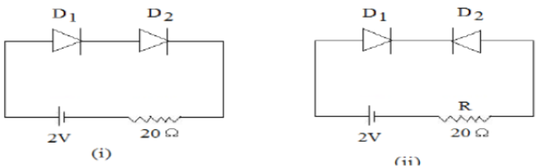
Answer:
Let's analyze both circuits under the assumption that the diodes are ideal (having zero resistance in forward bias and infinite resistance in reverse bias):
**(i) For Circuit (i):**
Both diodes \( D_1 \) and \( D_2 \) are connected such that their p-sides are toward the positive terminal of the \( 2\text{ V} \) battery. Therefore, both \( D_1 \) and \( D_2 \) are **forward biased** and offer zero resistance. The total current \( I \) flowing through the \( 20\ \Omega \) resistor is calculated using Ohm's law: \[ I = \frac{V}{R} = \frac{2 \text{ V}}{20\ \Omega} = 0.1 \text{ A} \]
**(ii) For Circuit (ii):**
Diode \( D_1 \) is forward biased, but diode \( D_2 \) is connected in the opposite direction, making it **reverse biased**. A reverse-biased diode acts as an open switch and offers infinite resistance. Since the components are connected in series, the reverse-biased diode blocks all current flow in the entire loop. Therefore, the current \( I \) through the resistor is: \[ I = 0 \text{ A} \]
In simple words: (i) In the first circuit, both diodes point in the correct direction (forward bias), allowing current to flow freely. The current is \( 2 \text{ V} / 20 \ \Omega = 0.1 \text{ Ampere} \). (ii) In the second circuit, the second diode is placed backwards (reverse bias), which acts like an open switch and blocks the entire current, making \( I = 0 \).
Exam Tip: If the diodes are not mentioned as ideal and instead have a forward barrier potential (e.g., \( 0.7\text{ V} \) for Silicon), subtract this barrier drop from the battery voltage before calculating the current (\( I = \frac{V - V_d}{R} \)).
Page 8
Question 25. In the given block diagram of a receiver identify the boxes labelled as X and Y also write their functions.
Answer:
In the block diagram of a receiver:
- **Box X represents the Intermediate Frequency (IF) stage.**
- **Box Y represents the Power Amplifier.**
**Functions:**
- **Intermediate Frequency (IF) stage (X):** It shifts the high radio-frequency (RF) carrier wave received from the antenna down to a lower, fixed intermediate frequency. This makes it much easier and more efficient to amplify and filter the signal before sending it to the detector.
- **Power Amplifier (Y):** It enhances the power and strength of the recovered audio/video signal coming out of the detector stage, making it strong enough to drive the output device (such as a loudspeaker).
In simple words: Box X is the IF stage, which lowers the high-frequency radio signal to a standard middle frequency so it's easier to process. Box Y is the power amplifier, which boosts the final audio signal so it's loud enough to be heard through a speaker.
Exam Tip: Be precise with the names: "Intermediate Frequency (IF) stage" and "Power Amplifier". Explicitly explaining how each stage helps in signal processing is crucial for full marks.
Question 26. Write two factors justifying the need of modulation for transmission of a signal.
Answer:
Modulation is essential for transmitting low-frequency baseband signals over long distances due to the following two factors:
1. **Practicable Antenna Length:**
To transmit a signal efficiently, the height of the antenna must be of the order of one-quarter of the wavelength of the signal (\( L \approx \frac{\lambda}{4} \)). For an audio signal of frequency \( 20 \text{ kHz} \), the wavelength is \( \lambda = \frac{c}{\nu} = \frac{3 \times 10^8}{20 \times 10^3} = 15 \text{ km} \), which requires an antenna height of about \( 3.75 \text{ km} \) — an impossible structure to build. By modulating the signal onto a high-frequency carrier (e.g., \( 1 \text{ MHz} \), \( \lambda = 300 \text{ m} \)), the required antenna height reduces to a manageable \( 75 \text{ m} \).
2. **Effective Power Radiated by Antenna:**
The power \( P \) radiated by an antenna of length \( l \) is inversely proportional to the square of the wavelength of the transmitted signal: \[ P \propto \left(\frac{l}{\lambda}\right)^2 \] Since the wavelength \( \lambda \) of a low-frequency signal is very large, the power radiated by the antenna is extremely small. By modulating the signal onto a high-frequency carrier wave (which has a much smaller wavelength \( \lambda \)), the power radiated by the antenna increases dramatically, ensuring long-distance transmission.
In simple words: (1) Low-frequency signals have huge wavelengths, requiring antennas miles high to transmit. Modulation uses high-frequency waves with short wavelengths, making the required antenna size small and practical. (2) Shorter wavelengths allow antennas to radiate much more energy, preventing the signal from dying out over long distances.
Exam Tip: Presenting the mathematical relations \( L \approx \frac{\lambda}{4} \) and \( P \propto \left(\frac{l}{\lambda}\right)^2 \) is highly expected by examiners to validate your two points.
Question 27. Identify the logic gates marked ‘P’ and ‘Q’ in the given circuit. Write the truth table for the combination.
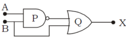
Answer:
- **Gate P is a NAND Gate.**
- **Gate Q is an OR Gate.**
The output of Gate P is \( Y_1 = \overline{A \cdot B} \).
The inputs to Gate Q are \( Y_1 \) and \( B \), so the final output \( X \) is: \[ X = B + \overline{A \cdot B} \] **Truth Table for the Combination:**
| Input A | Input B | Output of P (\( \overline{A \cdot B} \)) | Final Output \( X = B + \overline{A \cdot B} \) |
|---|---|---|---|
| 0 | 0 | 1 | 1 |
| 0 | 1 | 1 | 1 |
| 1 | 0 | 1 | 1 |
| 1 | 1 | 0 | 1 |
In simple words: Gate P is a NAND gate and Gate Q is an OR gate. No matter what combination of 1s and 0s you feed into inputs A and B, the final output of this circuit is always 1.
Exam Tip: Be sure to write the intermediate output of the NAND gate \( \overline{A \cdot B} \) in your truth table columns, which helps prevent mistakes and earns partial marks.
Question 28. State Kirchhoff s rules. Explain briefly how these rules are justified.
Answer:
Kirchhoff's rules for electrical networks are stated and justified below:
1. **Kirchhoff's First Rule (Junction Rule or Current Law):**
- **Statement:** In any electrical network, the algebraic sum of currents meeting at any junction point is always zero. This means the total current entering a junction equals the total current leaving it (\( \sum I_{\text{in}} = \sum I_{\text{out}} \)).
- **Justification:** This rule is based on the **law of conservation of charge**. Under steady current conditions, electric charge cannot accumulate or be depleted at any point or junction in the circuit; thus, whatever charge enters a junction per second must leave it.
2. **Kirchhoff's Second Rule (Loop Rule or Voltage Law):**
- **Statement:** The algebraic sum of changes in potential difference (voltages) across all elements (cells and resistors) around any closed loop in a circuit is always zero (\( \sum \Delta V = 0 \)).
- **Justification:** This rule is based on the **law of conservation of energy**. Since electrostatic force is conservative, the work done in moving a unit charge around any closed path must be zero. Consequently, the total gain in energy provided by the cells in a loop must equal the total energy dissipated across the resistors in that same loop.
In simple words: (1) The Junction Rule says whatever current goes into a crossroad must come out, because electric charges cannot vanish or build up at one spot (conservation of charge). (2) The Loop Rule says the total voltage supplied by batteries around any closed loop must equal the voltage used up by resistors, because the total energy in a closed loop remains constant (conservation of energy).
Exam Tip: Clearly link the Junction Rule to "conservation of charge" and the Loop Rule to "conservation of energy." These exact pairing phrases are the key targets of marking schemes.
Free study material for Physics
CBSE Class 12 Physics Worksheets for 2 Mark Question Bank
Download Chapter Worksheets: Class 12 Physics
Explore reliable practice questions for 2 Mark Question Bank tailored for Class 12 Physics learners. Use these structured worksheets to evaluate exam preparedness and strengthen problem-solving skills throughout the 2026 academic session.
Concept Clarification for 2 Mark Question Bank
Designed around the official curriculum for Class 12 Physics, these practice sheets guarantee standard compliance. Reviewing step-by-step solutions after completion sharpens your accuracy and clarifies complex sub-topics within 2 Mark Question Bank.
Effective Revision Strategies for School Exams
Follow up your worksheet practice by attempting the interactive online MCQ tests for 2 Mark Question Bank to evaluate your execution speed. All printable assignments and revision sheets on our platform are updated for the 2026 session and available free of charge.
FAQs
You can download the latest chapter-wise printable worksheets for Class 12 Physics 2 Mark Question Bank for free from StudiesToday.com. These have been made as per the latest CBSE curriculum for this academic year.
Yes, Class 12 Physics worksheets for 2 Mark Question Bank focus on activity-based learning and also competency-style questions. This helps students to apply theoretical knowledge to practical scenarios.
Yes, we have provided solved worksheets for Class 12 Physics 2 Mark Question Bank to help students verify their answers instantly.
Yes, our Class 12 Physics test sheets are mobile-friendly PDFs and can be printed by teachers for classroom.
For 2 Mark Question Bank, regular practice with our worksheets will improve question-handling speed and help students understand all technical terms and diagrams.