
Access the latest CBSE Class 12 Physics Semiconductor Devices And Communication System Worksheet. We have provided free printable Class 12 Physics worksheets in PDF format, specifically designed for Chapter 14 Semiconductor Electronics Materials Devices and Simple Circuits. These practice sets are prepared by expert teachers following the 2025-26 syllabus and exam patterns issued by CBSE, NCERT, and KVS.
Chapter 14 Semiconductor Electronics Materials Devices and Simple Circuits Physics Practice Worksheet for Class 12
Students should use these Class 12 Physics chapter-wise worksheets for daily practice to improve their conceptual understanding. This detailed test papers include important questions and solutions for Chapter 14 Semiconductor Electronics Materials Devices and Simple Circuits, to help you prepare for school tests and final examination. Regular practice of these Class 12 Physics questions will help improve your problem-solving speed and exam accuracy for the 2026 session.
Download Class 12 Physics Chapter 14 Semiconductor Electronics Materials Devices and Simple Circuits Worksheet PDF
Question. In a p-type semiconductor the acceptor level is situated 60 meV above the valence band. The maximum wavelength of light required to produce a hole will be
(a) 0.207 × 10⁻⁵ m
(b) 2.07 × 10⁻⁵ m
(c) 20.7 × 10⁻⁵ m
(d) 2075 × 10–5 m
Answer: B
Question. Pure Si at 500K has equal number of electron (ne) and hole (nh) concentrations of 1.5 × 10¹⁶ m–3. Doping by indium increases nh to 4.5 × 10²² m–3. The doped semiconductor is of
(a) n–type with electron concentration ne = 5 × 10²² m–3
(b) p–type with electron concentration ne = 2.5 ×10¹⁰ m–3
(c) n–type with electron concentration ne = 2.5 × 10²³ m–3
(d) p–type having electron concentration ne = 5 × 10⁹ m–3
Answer: D
Question. In insulator
(a) valence band is partially filled with electrons
(b) conduction band is partially filled with electrons
(c) conduction band is filled with electrons and valence band is empty
(d) conduction band is empty and valence band is filled with electrons.
Answer: D
Question. Symbolic representation of four logic gate are shown as
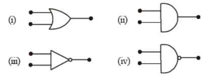
Pick out which ones are for AND, NAND and NOT gates, respectively
(a) (ii), (iii) and (iv)
(b) (iii), (ii) and (i)
(c) (iii), (iii) and (iv)
(d) (ii), (iv) and (iii)
Answer: D
Question. Distance between body centred atom & a corner atom in sodium(a = 4.225 Å) is
(a) 3.66 Å
(b) 3.17 Å
(c) 2.99 Å
(c) 2.54 Å
Answer: A
Question. In a triode, gm = 2 × 10⁻³ ohm–1 ; μ = 42; resistance of load, R = 50 kilo ohm. The voltage amplification obtained from this triode will be
(a) 30.42
(b) 29.57
(c) 28.18
(d) 27.15
Answer: B
Question. Zener diode is used for
(a) amplification
(b) rectification
(c) stabilisation
(d) all of the above
Answer: C
Question. Which one is the weakest type of bonding in solids ?
(a) Ionic
(b) Covalent
(c) Metallic
(d) Vander Wall’s
Answer: D
Question. A transistor has β = 40. A change in base current of 100 μ A, produces change in collector current
(a) 40 × 100 microampere
(b) (100 – 40) microampere
(c) (100 + 40) microampere
(d) 100/40 microampere
Answer: A
Question. In the energy band diagram of a material shown below, the open circles and filled circles denote holes and electrons respectively. The material is
(a) an insulator
(b) a metal
(c) an n-type semiconductor
(d) a p-type semiconductor
Answer: D
Question. Choose the only false statement from the following.
(a) In conductors, the valence and conduction bands may overlap.
(b) Substances with energy gap of the order of 10 eV are insulators.
(c) The resistivity of a semiconductor increases with increase in temperature.
(d) The conductivity of a semiconductor increases with increase in temperature.
Answer: C
Question. The current gain of a transistor in common base mode is 0.995. The current gain of the same transistor in common emitter mode is
(a) 197
(b) 201
(c) 198
(d) 199
Answer: D
Question. In forward biasing of the p–n junction
(a) the positive terminal of the battery is connected to p–side and the depletion region becomes thick
(b) the positive terminal of the battery is connected to n–side and the depletion region becomes thin
(c) the positive terminal of the battery is connected to n–side and the depletion region becomes thick
(d) the positive terminal of the battery is connected to p–side and the depletion region becomes thin
Answer: D
Question. If a small amount of antimony is added to germanium crystal
(a) it becomes a p–type semiconductor
(b) the antimony becomes an acceptor atom
(c) there will be more free electrons than holes in the semiconductor
(d) its resistance is increased
Answer: C
Question. By increasing the temperature, the specific resistance of a conductor and a semiconductor
(a) increases for both
(b) decreases for both
(c) increases, decreases
(d) decreases, increases
Answer: C
Question. At absolute zero, Si acts as
(a) non-metal
(b) metal
(c) insulator
(d) none of these
Answer: C
Question. On doping germanium with donor atoms of density 1017 cm–3 its conductivity in mho/cm will be
[Given : μe = 3800 cm2/V–s and ni = 2.5 × 1013 cm–13]
(a) 30.4
(b) 60.8
(c) 91.2
(d) 121.6
Answer: B
Question. The energy band gap is maximum in
(a) metals
(b) superconductors
(c) insulators
(d) semiconductors.
Answer: C
Question. In a npn transistor 1010 electrons enter the emitter in 10–6 s. 4% of the electrons are lost in the base. The current transfer ratio will be
(a) 0.98
(b) 0.97
(c) 0.96
(d) 0.94
Answer: C
Question. A transistor has a base current of 1 mA and emitter current 90 mA. The collector current will be
(a) 90 mA
(b) 1 mA
(c) 89 mA
(d) 91 mA
Answer: C
ONE MARKS QUESTIONS
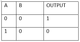
Question. Draw the truth table for a NOR gate.
Answer :
Question. Which diode is used for voltage regulation? Give its symbol.
Answer : Zener diode (Image 1)
Question. Draw the logic symbol for a NAND gate.
Answer :
Question. Which biasing will make the resistance of p-n junction high?
Answer : Reverse biasing
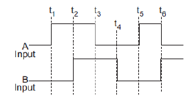
Question. In the given diagram, is the diode D forward or reverse biased?
Answer : Reverse biased
TWO MARKS QUESTIONS
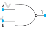
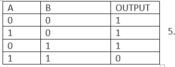
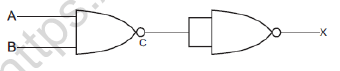
Question. Identify the equilent logic gate for the given logic gates. Write down the truth table for the final output of the combination.
Answer : NAND gate
Question. Explain how the depletion region and barrier potential are formed in a p-n junction diode.
Answer : Formation of Depletion Layer: At the junction there is diffusion of electrons of n-region to p-region while holes of p-region diffuse into n-region. Some electrons combine with holes to neutralise each other. Thus near the junction there is an excess of positively charged ions in n-region and an excess of negatively charged ions in p-region. This sets up a potentialdifference and hence an internal electric field Ei (junction field) across the junctions. The field Eiis directed from n-region to p-region.
Question. Draw the circuit diagram of a n-p-n common emitter transistor as an amplifier with proper biasing.If a change of 0.4 mA in base current causes a change of 10mA in collector current in a common emitter amplifier, find a.c.current gain of the transistor.
Answer : ß= change in collector current/change in base current = 25
THREE MARKS QUESTIONS
Question. Draw energy band diagram for a (i) p- type extrinsic semiconductor (ii) n-type extrinsic semiconductor (iii) intrinsic semiconductors.
Answer : (Image 4) .(i) p-type semiconductor
Question. Define the terms ‘potential barrier’ and ‘depletion region’ for a p-n junction diode. State how the thickness of depletion region will change when the p.n junction diode is (i) forward biased. (ii) Reverse biased.
Answer : Potential barrier-The loss of electrons from the n-region and the gain of electron by the p-region cause a difference of potential across the junction of the two regions. Since this potential tends to prevent the movement of electron from the n region into the p region, it is often called a barrier potential.
Depletion region- The space-charge region on either side of the junction which is free of electrons and holes is known as depletion region.
(i) Thickness of depletion region decreases when diode is forward biased.
(ii) Thickness of depletion region increases when diode is reverse biased.
Question.With the help of labeled circuit diagram, explain the rectification action of a full wave rectifier.
Answer : Answer included in 10 years question answer.
Question.Distinguish between conductors, semiconductors and insulators on the basis of band theory of solids.
Answer : In metal either the conduction band is partially filled and the balanced band is partially empty or the conduction and valance bands overlap. When there is overlap electrons from valence band can easily move into the conduction band. This situation makes a large number of electrons available for electrical conduction. When the valence band is partially empty, electrons from its lower level can move to higher level making conduction possible (Image 4)
This situation is shown in Fig.(c). Here a finite but small band gap (Eg< 3 eV) exists. Because of the small band gap, at room temperature some electrons from valence band can acquire enough energy to cross the energy gap and enter the conduction band. These electrons (though small in numbers) can move in the conduction band.
In this case, as shown in Fig.(b), a large band gap Egexists (Eg> 3 eV). There are no electrons in the conduction band, and therefore no electrical conduction is possible. Note that the energy gap is so large that electrons cannot be excited from the valence band to the conduction band by thermal excitation. This is the case of insulators.
22
Please click on below link to download CBSE Class 12 Physics Semiconductor Devices And Communication System Worksheet
Free study material for Physics
Chapter 14 Semiconductor Electronics Materials Devices and Simple Circuits CBSE Class 12 Physics Worksheet
Students can use the Chapter 14 Semiconductor Electronics Materials Devices and Simple Circuits practice sheet provided above to prepare for their upcoming school tests. This solved questions and answers follow the latest CBSE syllabus for Class 12 Physics. You can easily download the PDF format and solve these questions every day to improve your marks. Our expert teachers have made these from the most important topics that are always asked in your exams to help you get more marks in exams.
NCERT Based Questions and Solutions for Chapter 14 Semiconductor Electronics Materials Devices and Simple Circuits
Our expert team has used the official NCERT book for Class 12 Physics to create this practice material for students. After solving the questions our teachers have also suggested to study the NCERT solutions which will help you to understand the best way to solve problems in Physics. You can get all this study material for free on studiestoday.com.
Extra Practice for Physics
To get the best results in Class 12, students should try the Physics MCQ Test for this chapter. We have also provided printable assignments for Class 12 Physics on our website. Regular practice will help you feel more confident and get higher marks in CBSE examinations.
FAQs
You can download the teacher-verified PDF for CBSE Class 12 Physics Semiconductor Devices And Communication System Worksheet from StudiesToday.com. These practice sheets for Class 12 Physics are designed as per the latest CBSE academic session.
Yes, our CBSE Class 12 Physics Semiconductor Devices And Communication System Worksheet includes a variety of questions like Case-based studies, Assertion-Reasoning, and MCQs as per the 50% competency-based weightage in the latest curriculum for Class 12.
Yes, we have provided detailed solutions for CBSE Class 12 Physics Semiconductor Devices And Communication System Worksheet to help Class 12 and follow the official CBSE marking scheme.
Daily practice with these Physics worksheets helps in identifying understanding gaps. It also improves question solving speed and ensures that Class 12 students get more marks in CBSE exams.
All our Class 12 Physics practice test papers and worksheets are available for free download in mobile-friendly PDF format. You can access CBSE Class 12 Physics Semiconductor Devices And Communication System Worksheet without any registration.