UNIT-9
ELECTRONIC DEVICES
1.What is the order of energy gap in a conductor, semi conductor, and insulator?.
2.Why does the conductivity of a semi conductor change with the rise in temperature ?
3. Is the number of electrons greater than, less than (or) equal to the number of holes in an intrinsic semi conductor?
4.Show in a energy band diagram the donor level for an N-type semi conductor.
5.. Draw in a energy band the acceptor level for a P-type semi conductor .
6.what is knee voltage in a junction Diode?
7. In transistor a current controlled (or)temperature controlled device?.
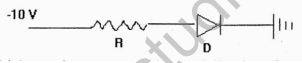
8. In a given diagram ,is the diode reverse (or) forward biased?.
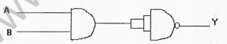
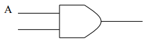
9.which gate is represented by the following diagram?.
10.The ratio of number of free electrons to holes ne/nh for two different materials A and B are 1 and <1 respectively. Name the type of semi conductor to which A and B belongs.
11.In half wave rectification , what is the output frequency if the input frequency is 50 hz. What is the output frequency of a full wave rectification for the same input frequency.
12. How can you relate drift velocity and mobility of an electron?
13. Show by the graph how does the current vary with the voltage change for a junction diode.
14. Why do semiconductors obey OHM’S law for only low fields?
15. Mention the factors upon which Tranconductance of a transistor depend.
16. For faster action which transistor is used and why?
17. What are input and output characteristics of a transistor? Draw the graphs.
Ans:
18. A germanium diode is preferred to a silicon one for rectifying small voltages. Explain why?
Ans: Because the energy gap for Ge ( Eg = 0.7 ev) is smaller than the energy gap for Si (Eg = 1.1ev ) . Moreover, the germanium diode is much more open to the danger of high temperature affect than silicon at high voltage.
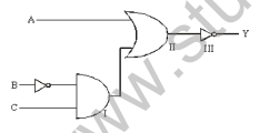
19.Express by a truth table the output Y for all possible inputs A and B in the circuit shown below.
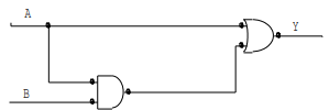
20. Write the Boolean equation and truth table for the circuit shown below.What is the output when all the inputs are high?
21) Construct AND gate using NAND GATE and give its truth table.
23. For a common emitter amplifier, current gain = 50. If the emitter current is 6.6mA, calculate collector and base current. Also calculate current gain, when emitter is working as common base amplifier.
24.The base current is 100μA and collector current is 3mA.
a) Calculate the values of b, Ie, and a
b) A change of 20μA in the base current produces a change of 0.5mAin the collector current. Calculate ba.c.
25. In NPN transistor circuit, the collector current is 5mA. If 95% of the electrons emitted reach the collector region,what is the base current?
Ans: Here
Ic=95% of Ie = (95 / 100 ) Ie
Ie = (100 / 95) × 5 mA = 5.26mA
Ie= Ic+ Ib
Ib = 0.25 mA
26. In a transistor circuit shown the figure, the emitter current is 5mA and collector current 4.75 mA. Calculate the base current and the value of Rb.
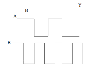
27.A circuit symbol of a logic gate and two input wave forms A and B are shown.
a) Name the logic gate
b) Give the output wave form
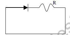
28. The diode shown in the figure has a constant voltage drop of 0.5V at all currents and a maximum power rating of 100mW. What should be the value of resistance R connected in series,
for maximum current.?
29.For a transistor working as a common base amplifier, current gain is 0.96. If the emitter current is 7.2mA, then calculate the base current.
30. For a common emitter amplifier, the current gain is 70. If the emitter current is 8.8mA, calculate the collector and base current.
31.The base current of a transistor is 105 μA and collector current is 2.05 mA.
a) Deterine the value of b , Ie , and a
b) A change of 27 μA in the base current produces a change of 0.65 mA in the collector current . Find ba.c.
32. In a silicon transistor, a change of 7.89mA in the emitter current produces a change of 7.8 mA in the collector current. What change in the base current is necessary to produce an equivalent change in the collector current?
ADDITIONAL QUESTIONS
(1) Out of electrons and holes, which has higher mobility?
(2) Which special type of diode can act as a voltage regulator? Give the symbol of this diode and draw the general shape of its V-I characteristics.
(3) What do you mean by rectification?
(4) If a semiconductor has an intrinsic carrier concentration 1.04x10¹⁴/m3 of when doped with 1023/m3phosphorous atoms, calculate the concentration of hole/m3 at room temperature .
(5) In a common emitter circuit, if VCE is changed by 0.5 V, collector current Changes by 0.002 mA. What is the output resistance?
(6) Name the electrical circuits used to get smooth D.C. output from a rectified circuit.
(7) How does the energy gap of an intrinsic semiconductor vary when doped with a trivalent impurity?
(8) Draw energy band diagram of n-type semiconductor.
(9) A semiconductor has equal electron and hole concentration 6×10⁸ /m3 .On doping with a certain impurity, electron concentration increases to 8×10¹² /m3 .Identify the type of
semiconductor after doping.
(10) How does the dc current gain of a transistor change, if the width of the base region is increased?
(11) Why are photodiodes used preferably in reverse bias condition?
2 marks questions
(1) In the working of a transistor, emitter base junction is forward biased, while the collector base junction is reverse biased, why: To make transistor to act as an amplifier.
(2) In a transistor base is lightly doped and is a thin layer, why? To reduce the neutralization in the base emitter junction.
(3)What is the condition for the state of saturation of a transistor?
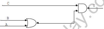
(4)Write the truth table for the following logic circuit shown in the figure below.
3 marks questions
(1) Discuss how the OR gate is realized from the NOR gate.
(2) Why is the base region of a transistor usually made thin?In a common emitter mode of transisitor, d.c. current gain is 20, the emitter current is 7 mA. Calculate (i) base current,
and (ii) collector current.
(3) The input resistance of a silicon transistor is 665 Ω. Its base current is changed by 15 μA, which results in change of collector current by 2mA. This transistor is used as a common emitter amplifier with a load resistance of 5 k .
Calculate (i) current gain ,
(ii) transconductance gm, and (iii) voltage gain Av of the amplifier.
(4) Draw the energy band diagram of a p-type semiconductor. Distinguish between p-type and n-type semiconductor.
(5)Explain briefly with the help of a circuit, how V-I characteristics of a p-n junction diode are obtained in (a) Forward bias (b) Reverse bias. Draw the shape of curves obtained.
(6)In a common emitter transistor amplifier, the input resistance of a transistor is 100 ohm. On changing its base current by 10μA, the collector current increases by 2mA.If a load
resistance of 5kilo ohm is used in the circuit, calculate (a) current gain (b) voltage gain of the amplifier
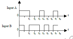
(7) Two signals A, B as given below, are applied as input to
(i) AND (ii) NOR and
(iii) NANDgates. Draw the output wave-form in each case.
5 marks questions
(1) Draw a circuit diagram to obtain the characteristics of a n-p-n transistor in common emitter configuration. Describe how you will obtain input and output characteristics.
Give shape of the curves.
(2) Explain the function of base region of a transistor. Draw a circuit diagram to study the input and output characteristics of NPN transistor in a common emitter (CE) configuration. Show these characteristics graphically. Explain how the current amplification factor is calculated from these characteristics.
(3) Explain the working of transistor as an oscillator with the help of a neat diagram.
(4) A student has to study the input and output characteristics of a n-p-n silicon transistor in the Common Emitter configuration. What kind of a circuit arrangement should she use for this purpose? Draw the typical shape of input characteristics likely to be obtained by her. What do we understand by the cut off, active and saturation states of the transistor? In which of these states does the transistor not remain when being used as a switch?
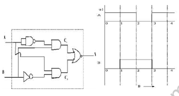
(5) Input signals A and B are applied to the input terminals of the ‘dotted box’ set-up shown here. Let Y be the final output signal from the box. Draw the wave forms of the signals labeled as C1 and C2 within the box, giving (in brief) the reasons for getting these wave forms. Hence draw the wave form of the final output signal Y. Give reasons for your choice. What can we state (in words) as the relation between the final output signal Y and the input signals A and B?