
Refer to CBSE Class 12 Physics HOTs Semiconductor Electronics Materials and Devices and Simple Circuits. We have provided exhaustive High Order Thinking Skills (HOTS) questions and answers for Class 12 Physics Chapter 14 Semiconductor Electronics Materials Devices and Simple Circuits. Designed for the 2026-27 exam session, these expert-curated analytical questions help students master important concepts and stay aligned with the latest CBSE, NCERT, and KVS curriculum.
Chapter 14 Semiconductor Electronics Materials Devices and Simple Circuits Class 12 Physics HOTS with Solutions
Practicing Class 12 Physics HOTS Questions is important for scoring high in Physics. Use the detailed answers provided below to improve your problem-solving speed and Class 12 exam readiness.
HOTS Questions and Answers for Class 12 Physics Chapter 14 Semiconductor Electronics Materials Devices and Simple Circuits
.
SEMICONDUCTOR DEVICES
ONE MARKS QUESTIONS
Question. What type of biasing is used to operate a photo diode?
Answer : Reverse bias
Question. Why is n-p-n transistor preferred over p-n-p transistor?
Answer : Electrons are the majority charge carriers in n-p-n transistor and electrons have higher mobility than holes.
Question. How does the energy gap in an intrinsic semiconductor vary, when doped with a trivalent impurity?
Answer : decreases.
Question. How does conductivity of a semiconductor change with rise in its temperature?
Answer : increases
Question. What is the order of energy gap in a semiconductor?
Answer : Approx. 1eV
TWO MARKS QUESTIONS
Question. How does the collector current change in a junction transistor, if the base region has larger width?
Answer : As we know
If we increase base width region there is more recombination in the base region. So base current(Ib) will increase. Hence, the collector current decreases if emitter current (Ie) is fixed for a transistor
Question. What is meant by the term, doping of an intrinsic semiconductor? How does it affect the conductivity of a semiconductor?
Answer : Adding impurities-trivalent or pentavalent, conductivity increases
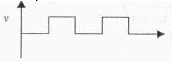
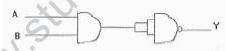
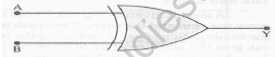
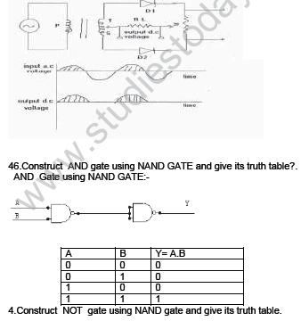
Question. If the output of NAND gate is fed into the input to a NOT gate (i) name the new logic gate obtained and (ii) write down its truth table.
Answer : 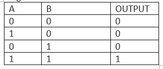
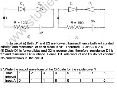
Question. How does the width of the depletion region of a p-n junction vary, when diode is (i) forward biased (ii) Reverse biased?
Answer : (i) decreases (ii) increases:-
THREE MARKS QUESTIONS
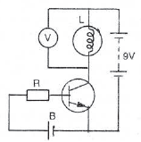
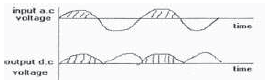
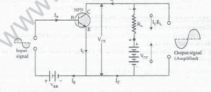
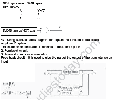
Question.Draw the circuit diagram of a common-emitter amplifier, with appropriate biasing. What is the phase difference between the input and output signals? State two reasons why a common-emitter-amplifier is preferred to a common base amplifier?
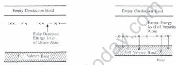
Answer : In this case, as shown in Fig.(b), a large band gap Egexists (Eg> 3 eV). There are no electrons in the conduction band, and therefore no electrical conduction is possible. Note that the energy gap is so large that electrons cannot be excited from the valence band to the conduction band by thermal excitation. This is the case of insulators.
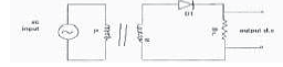
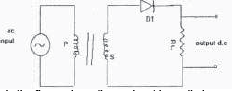
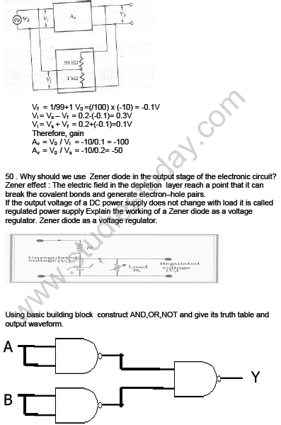
Question. With a circuit diagram, briefly explain how a zener diode can be used as a voltage regulator.
Answer : Answer included in 10 years question answer
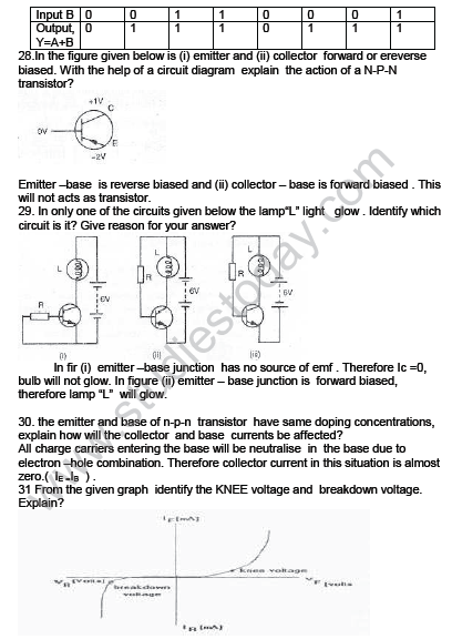
Question. The V-I characteristic of a silicon diode is shown in the Fig. Calculate the resistance of the diode at (a) ID= 15 mA and (b) VD= –10 V.
Answer : Considering the diode characteristics as a straight line between I = 10 mA to I = 20 mA passing through the origin, we can calculate the resistance using Ohm’s law.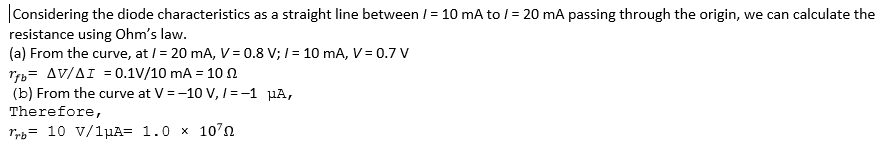
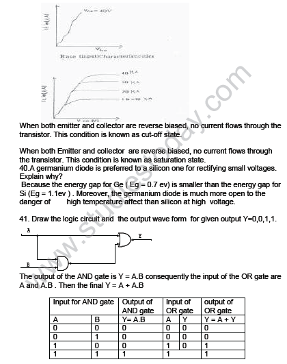
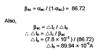
Question. From the output characteristics shown in Fig, calculate the values ofac and dc of the transistor when VCE is10 V and IC = 4.0 mA.
Answer : 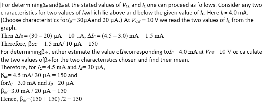
Answer :
Answer :


Answer :
Answer :

Free study material for Physics
HOTS for Chapter 14 Semiconductor Electronics Materials Devices and Simple Circuits Physics Class 12
Students can now practice Higher Order Thinking Skills (HOTS) questions for Chapter 14 Semiconductor Electronics Materials Devices and Simple Circuits to prepare for their upcoming school exams. This study material follows the latest syllabus for Class 12 Physics released by CBSE. These solved questions will help you to understand about each topic and also answer difficult questions in your Physics test.
NCERT Based Analytical Questions for Chapter 14 Semiconductor Electronics Materials Devices and Simple Circuits
Our expert teachers have created these Physics HOTS by referring to the official NCERT book for Class 12. These solved exercises are great for students who want to become experts in all important topics of the chapter. After attempting these challenging questions should also check their work with our teacher prepared solutions. For a complete understanding, you can also refer to our NCERT solutions for Class 12 Physics available on our website.
Master Physics for Better Marks
Regular practice of Class 12 HOTS will give you a stronger understanding of all concepts and also help you get more marks in your exams. We have also provided a variety of MCQ questions within these sets to help you easily cover all parts of the chapter. After solving these you should try our online Physics MCQ Test to check your speed. All the study resources on studiestoday.com are free and updated for the current academic year.
FAQs
You can download the teacher-verified PDF for CBSE Class 12 Physics HOTs Semiconductor Electronics Materials and Devices and Simple Circuits from StudiesToday.com. These questions have been prepared for Class 12 Physics to help students learn high-level application and analytical skills required for the 2026-27 exams.
In the 2026 pattern, 50% of the marks are for competency-based questions. Our CBSE Class 12 Physics HOTs Semiconductor Electronics Materials and Devices and Simple Circuits are to apply basic theory to real-world to help Class 12 students to solve case studies and assertion-reasoning questions in Physics.
Unlike direct questions that test memory, CBSE Class 12 Physics HOTs Semiconductor Electronics Materials and Devices and Simple Circuits require out-of-the-box thinking as Class 12 Physics HOTS questions focus on understanding data and identifying logical errors.
After reading all conceots in Physics, practice CBSE Class 12 Physics HOTs Semiconductor Electronics Materials and Devices and Simple Circuits by breaking down the problem into smaller logical steps.
Yes, we provide detailed, step-by-step solutions for CBSE Class 12 Physics HOTs Semiconductor Electronics Materials and Devices and Simple Circuits. These solutions highlight the analytical reasoning and logical steps to help students prepare as per CBSE marking scheme.