
Refer to CBSE Class 12 Physics HOTs Conductor. We have provided exhaustive High Order Thinking Skills (HOTS) questions and answers for Class 12 Physics Chapter 14 Semiconductor Electronics Materials Devices and Simple Circuits. Designed for the 2026-27 exam session, these expert-curated analytical questions help students master important concepts and stay aligned with the latest CBSE, NCERT, and KVS curriculum.
Chapter 14 Semiconductor Electronics Materials Devices and Simple Circuits Class 12 Physics HOTS with Solutions
Practicing Class 12 Physics HOTS Questions is important for scoring high in Physics. Use the detailed answers provided below to improve your problem-solving speed and Class 12 exam readiness.
HOTS Questions and Answers for Class 12 Physics Chapter 14 Semiconductor Electronics Materials Devices and Simple Circuits
Section: A
Very short answer question
Question. What is the order of energy gap in a conductor, semi conductor, and insulator?.
Answer: Conductor - no energy gap
Semi Conductor - It is of the order of 1 ev.
Insulator - 6 ev (or) more than 6 ev.
Question. Zener effect and avalanche effect are the two possible break down mechanisms that helps the external current . Why
Answer: Zener effect : The electric field in the depletion layer reach a point that it can break the covalent bonds and generate electron–hole pairs.
Avalanche breakdown : The minority carriers that across the depletion layer under the influence of the electric field gain sufficient kinetic energy to be able to break covalent bond in atoms which they collide.
Question. Light emission in semiconductor is the process of creation of a photon by means of the annihilation of an electron-hole pair. How can we create them. Give the necessary condition for the light emission?
Answer: hυ = Eeh greater than or equal to Eg.
Question. Why does the conductivity of a semi conductor change with the rise in temperature ?
Answer: When a semi conductor is heated more & more electrons get enough energy to jump across the forbidden energy gap from valence band to the conduction band, where they are free to conduct electricity. Thereby increasing the conductivity of a semi conductor.
Question. On the basis of energy level diagram, identify the P-type semi conductor & N-type semi conductor
Answer: 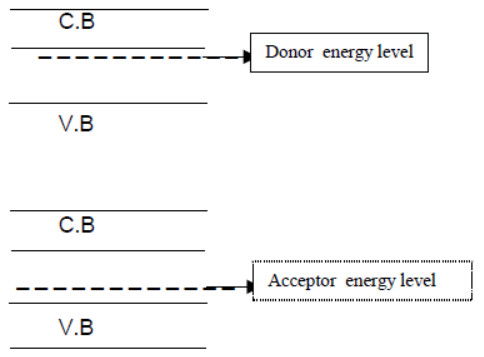
Question. A student has to study the characteristics of a P-N Junction diode. What kind of a circuit arrangement should she use for this purpose?
Answer: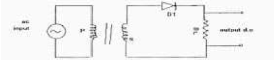
Question. Draw the typical shape of input characteristics likely to be obtainedby a student .
What do we understand by the forward bias and reverse bias of the diode? In which of these states does the diode being used as a rectifier.?
Answer: 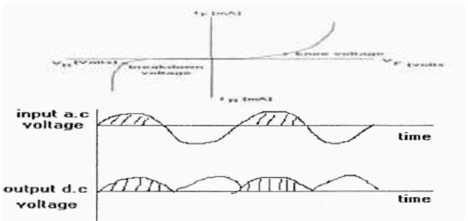
Question. To achieve light amplification, We should provide positive feed back in LASER .Why?
Answer: Laser is not an amplifier but an oscillator! However, any oscillator is an amplifier with a positive feedback. To obtain lasing , it is necessary to achieve light amplification and provide positive optical feedback.
Question. Self supporting stimulated emission is the principle of a Laser .why?
Answer: Probability of stimulated emission is proportional to the density of excess electrons and holes , and to the density of photons. Under the normal circumstances it is negligible. Therefore if we provide a positive feedback , the stimulated emission can become self supporting.
Question. If the active layer in a P-N photo diode is the thick depletion layer then P-N Photodiode act very effective . Why?
Answer: In p-I-n photodiode ,due to thick i – layer the sensitivity improves dramatically.. Large reverse biases (< 100V for Si ) may be required.
Question. Modern technology use poly silicon instead of metal to form the gate. Why?
Answer: Poly silicon has high conductivity compare to metal.
Question. Digiatal signal is preferred for communication Why not analog signal?Give its waveform.
Answer: A continuous time varying wave form of a current (or) voltage is called analogue signal. 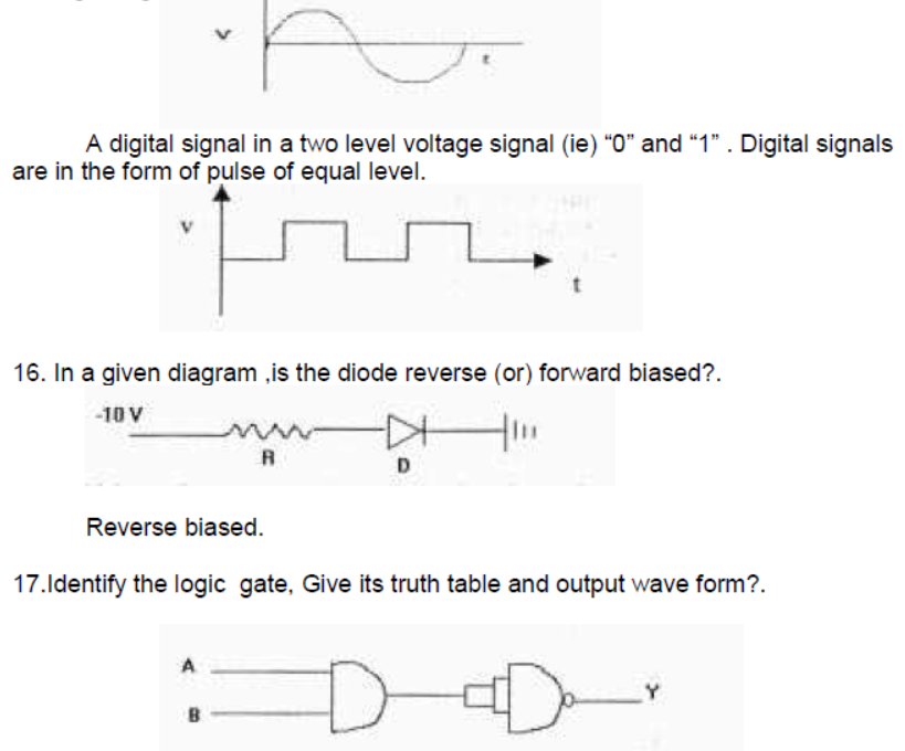
Question. The ratio of number of free electrons to holes ne/nh for two different materials A and B are 1 and <1 respectively. Name the type of semi conductor to which A and B belongs.
Answer: If ne/nh =1 . Hence A is intrinsic semi conductor.
If ne/nh <1 , ne<nh hence B is P-type.
Question. Can you identify waveform. How will you convert A.C To D.C?
Answer: 
Question. Under what conditions an amplifier can be converted in to an oscillator.Draw a suitable diagram .
Answer: 1. When feed back is positive. 2. When feed factor k is equal to l/AV 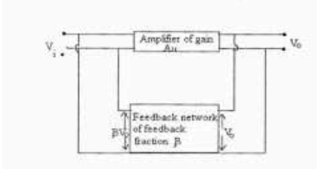
Question. Using basic logic gates (NOT, OR, AND ) construct the circuit for the given logic gate & give its truth table and wave form.?
Answer: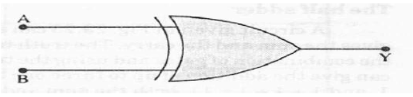
Question. Convert a Fraction from Decimal (0.625)10 to Binary?
Answer: (0.625)10 = (0.101)2
Question. Convert an octal number (4536) into decimal number?
Answer: (4536)8 = 4 x 83 + 5 x 82 + 3 x 81 + 6 x 80 = (1362)10
Question. Convert Hexa decimal (3A9F) and (2D3.5) into decimal number?
Answer: (3A9F)16 = 3x163 + 10x162 + 9x161 + 15x160 = 1499910
(2D3.5)16 = 2x162 + 13x161 + 3x160 + 5x16-1 = 723.312510
Question. In the circuit diagram given , a volt meter is connected across a lamp , what changes would occur at lamp”L” and voltmeter “V:” , if the resistor R is reduce in value? Give reason for your answer?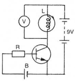
Answer: In the given circuit emitter –base junction of N-P-N transistor is forward biased , with battery “B”. When “r” decreases IE increases . Because
IC = IE – IB .
Therefore IC will also increase. Hence bulb will glow with more brightness and voltmeter reading will increase.
SHORT ANSWER QUESTIONS [ 2-MARKS]
Question. Determine the current through resistance “R” in each circuit. Diodes D1 and D2 are identical and ideal. 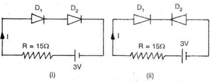
Answer: In circuit (i) Both D1 and D2 are forward baiased hence both will conduct current and resistance of each diode is “0”. .Therefore I = 3/15 = 0.2 A
(ii) Diode D1 is forward bias and D2 is reverse bias, therefore resistance D1 is “0” and resistance D2 is infinite. Hence D1 will conduct and D2 do not conduct .
No current flows in the circuit.
Question. Write the output wave form of the OR gate for the inputs given?
Answer: 

Question. In the figure given below is (i) emitter and (ii) collector forward or ereverse biased. With the help of a circuit diagram explain the action of a N-P-N transistor?
Answer: (i) Emitter –base is reverse biased and (ii) collector – base is forward biased . This will not acts as transistor.
Question. In only one of the circuits given below the lamp“L” light glow . Identify which circuit is it? Give reason for your answer? 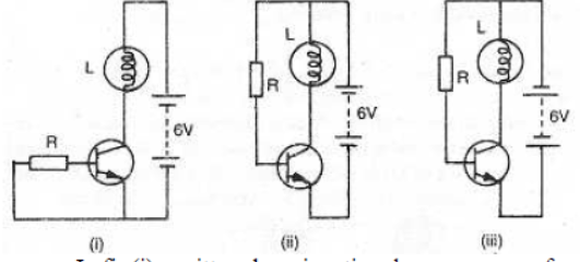
Answer: In fir (i) emitter –base junction has no source of emf . Therefore Ic =0, bulb will not glow. In figure (ii) emitter – base junction is forward biased, therefore lamp “L” will glow.
Question. the emitter and base of n-p-n transistor have same doping concentrations, explain how will the collector and base currents be affected?
Answer: All charge carriers entering the base will be neutralise in the base due to electron –hole combination. Therefore collector current in this situation is almost zero.( IE =IB ) .
Question. From the given graph identify the KNEE voltage and breakdown voltage. Explain?
Answer: 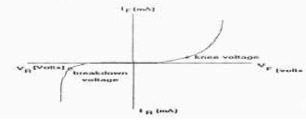
Question. Differentiate the electrical conductivity of both types of extrinsic semiconductors in terms of the energy band picture.
Answer: 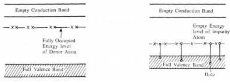
Question. semiconductors obey OHM’S law for only low fields .Give reason?
Answer: The drift velocity of a charge carrier is proportional to electric E.
Therefore V = eET/m ie. V α E
But V cannot be increased indefinitely by increasing E . At high speed relaxation time (T) begins to decrease due to increase in collision frequency. S: so drift velocity saturates at thermal velocity (lOms-1). An electric field of 106 V/m causes saturation of drift velocity. Hence semi- conduction obey ohm’s law for low electrical field and above this field ( E < 106 V/m ) current becomes independent of potential.
Question. Relate input frequency and the output frequencies of a half wave rectifier and a full wave rectifier?
Answer: In half-wave rectification, we get pulsating output for half cycle only.
Therefore output ripple frequency is same as the input frequency. But in full wave rectification we get output for both half cycle. Hence the output at ripple frequency is full-wave rectification is double the input frequency.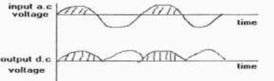
Question. Emitter is heavily doped while collector is moderately doped . Why?
Answer: There are two main differences between emitter and collector of a transistor construction wise. First emitter is heavily doped while collector is moderately doped. Second the area of the collector is larger than the emitter.So output will be maximum.
Question. Key point for its proper functioning of base region in a transistor depends upon the thickness of the base Why ?
Answer: Base region in a transistor controls the current. The majority charge carriers supplied by the emitter do not combine in the same region due to its thin size and light doping and most of them pass on to the collector. This is the key point for its proper functioning.
Question. For faster action which transistor is used and why?
Answer: For faster action NPN Transistor is used .In an NPN transistor, current conduction is mainly by free electron ,whereas in PNP type transistor .it is mainly holes Since electron are more mobile than holes we prefer NPN for faster action as well as high conduction current.
Question. A student has to study the input and output characteristics of a n-p-n silicon transistor in the common emitter configuration. What kind of a circuit arrangement should she use for this purpose?
Answer: 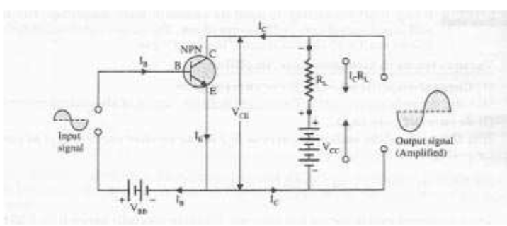
Question. Draw the typical shape of input characteristics likely to be obtained by a student.
Answer: What do we understand by the cut off, active and saturation of the transistor? In which of these states does the transistor not remain when being used as a switch?
When both emitter and collector are reverse biased, no current flows through the transistor. This condition is known as cut-off state.
When both Emitter and collector are reverse biased, no current flows through the transistor. This condition is known as saturation state.
Question. A germanium diode is preferred to a silicon one for rectifying small voltages. Explain why?
Answer: Because the energy gap for Ge ( Eg = 0.7 ev) is smaller than the energy gap for Si (Eg = 1.1ev ) . Moreover, the germanium diode is much more open to the danger of high temperature affect than silicon at high voltage.
Question. Draw the logic circuit and the output wave form for given output Y=0,0,1,1.
Answer: 
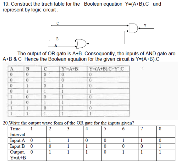
Question. Is it Logic gate used to prove Commutativity and Associativity ? Draw the truth table ?
Answer: The Commutative Property:
a + b = b + a
a · b = b · a
The Associative Property:
a + (b + c) = (a + b) + c
a · (b · c) = (a · b) · c
Section-C
SHORT ANSWER QUESTIONS [ 3-MARKS]
Question. Diode acts as rectifier Why? Differentiate between Half wave and full wave rectification?
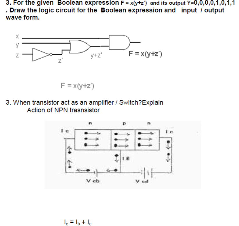
Answer: Rectification — It is the process in which alternating current is converted to direct current.P-N junction Diode as Half wave rectifier 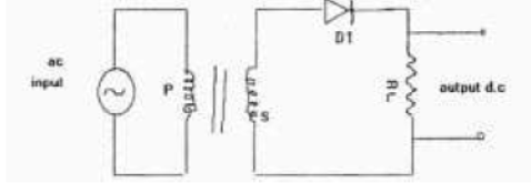
As shown in the figure above the a.c input is applied across the primary of transformer. The secondary is connected to junction diode and load resistance (Rc) in series.
WORKING PRINCIPLE:- when positive half cycle or a.c takes place the diode is forward biased and output is obtained across the load resistance Rc. But when it negative half cycle diode is reverse biased and no current flows, hence there is no output across load resistance Rc. So only half is obtained as output.
Full wave rectification: 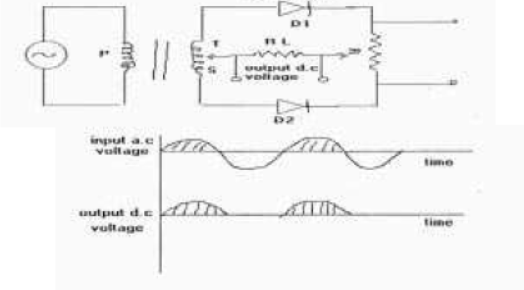
Question. Construct AND gate using NAND GATE and give its truth table?.
Answer: AND Gate using NAND GATE:- 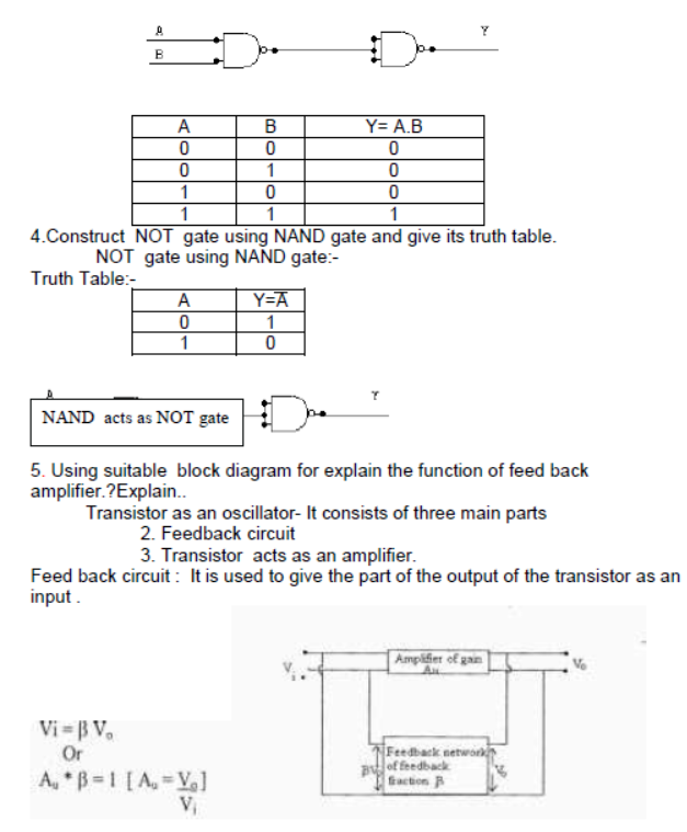
Transistor acts as an amplifier : in this circuit the NPN transistor acts as an amplifier. It amplifies the input signal. This amplified output goes to the Rl .
Question. Compliment(1’s) the following binary numbers
Answer: (a) 110010 (b) 111101 (c) 101010 (d)111111
(a) 1’s compliment=001101
(b) 1’s compliment=000010
(c) 1’s compliment=010101
(d) 1’s compliment=000000
Question. In the circuit, Vs=0.2V, V0 = -10 V. Find Vi & gain Av = V0 / Vi & Av ‘ = V0 / Vs ?
Answer: Vs=0.2 V, V0 = -10 V 
Vf = 1/99+1 V0 =(/100) x (-10) = -0.1V
Vi = Vs – Vf = 0.2-(-0.1)= 0.3V
Vi = Vs + Vf = 0.2+(-0.1)=0.1V
Therefore, gain
Av = V0 / Vi = -10/0.1 = -100
Av = V0 / Vs = -10/0.2= -50
SECTION- D
Long Answer Type Question [5-marks]
Question. Why should we use Zener diode in the output stage of the electronic circuit?
Answer: Zener effect : The electric field in the depletion layer reach a point that it can break the covalent bonds and generate electron–hole pairs.
If the output voltage of a DC power supply does not change with load it is called regulated power supply Explain the working of a Zener diode as a voltage regulator. Zener diode as a voltage regulator. 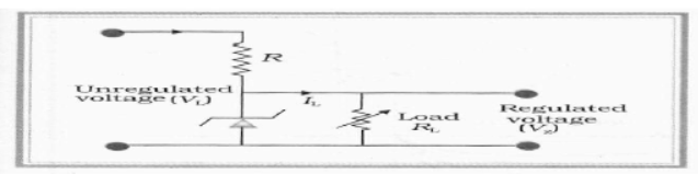
Question. Using basic building block construct AND,OR,NOT and give its truth table and output waveform.
Answer: 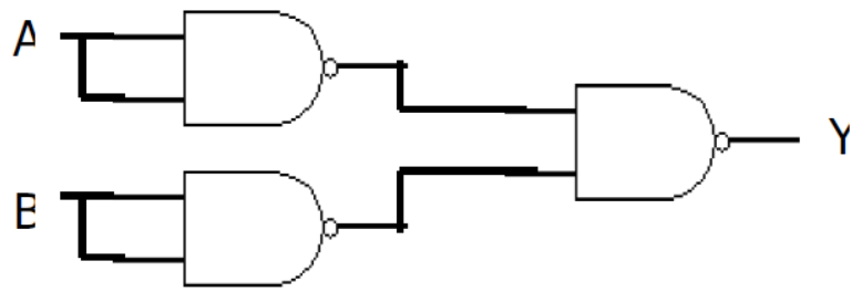
Question. The output of the transistor amplifier is 180º out of phase Why ?
Answer: CE Transistor acts as an amplifier:-
Using Kirchhoffs first law, IE = IB + IC
This voltage drop ICRL is clearly in opposition to the applied voltage Vcc.
Net collector voltage, VCE = Vcc - ICRL .. (1)
Question. Draw a circuit diagram for PNP common emitter transistor characteristics.
Explain the input and output characteristics.
Common Emitter Transistor characteristics.
Answer: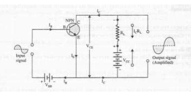
Output Characteristics of PNP represent the variation of collector current 1 with collector voltage Vce , keeping base constant current Ib. 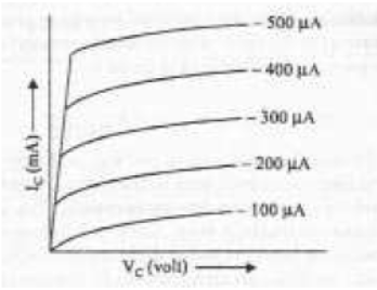
Question. Identify which basic gate OR, AND and NOT is represented by the circuits in the dotted lines boxes 1,2 and 3. Give the truth table for the entire circuit for all possible values of A and B?
Answer: 
SOLID AND SEMICONDUCTORS
Question. In NPN transistor circuit, the collector current is 5mA. If 95% of the electrons emitted reach the collector region, what is the base current?
Answer: Here
Ic=95% of Ie = (95 / 100 ) Ie
Ie = (100 / 95) × 5 mA = 5.26mA
Ie= Ic+ Ib
Ib = 0.25 mA
Question. A circuit symbol of a logic gate and two input wave forms A and B are shown.
Answer: 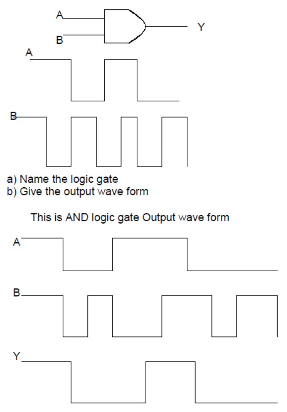

Free study material for Physics
HOTS for Chapter 14 Semiconductor Electronics Materials Devices and Simple Circuits Physics Class 12
Students can now practice Higher Order Thinking Skills (HOTS) questions for Chapter 14 Semiconductor Electronics Materials Devices and Simple Circuits to prepare for their upcoming school exams. This study material follows the latest syllabus for Class 12 Physics released by CBSE. These solved questions will help you to understand about each topic and also answer difficult questions in your Physics test.
NCERT Based Analytical Questions for Chapter 14 Semiconductor Electronics Materials Devices and Simple Circuits
Our expert teachers have created these Physics HOTS by referring to the official NCERT book for Class 12. These solved exercises are great for students who want to become experts in all important topics of the chapter. After attempting these challenging questions should also check their work with our teacher prepared solutions. For a complete understanding, you can also refer to our NCERT solutions for Class 12 Physics available on our website.
Master Physics for Better Marks
Regular practice of Class 12 HOTS will give you a stronger understanding of all concepts and also help you get more marks in your exams. We have also provided a variety of MCQ questions within these sets to help you easily cover all parts of the chapter. After solving these you should try our online Physics MCQ Test to check your speed. All the study resources on studiestoday.com are free and updated for the current academic year.
FAQs
You can download the teacher-verified PDF for CBSE Class 12 Physics HOTs Conductor from StudiesToday.com. These questions have been prepared for Class 12 Physics to help students learn high-level application and analytical skills required for the 2026-27 exams.
In the 2026 pattern, 50% of the marks are for competency-based questions. Our CBSE Class 12 Physics HOTs Conductor are to apply basic theory to real-world to help Class 12 students to solve case studies and assertion-reasoning questions in Physics.
Unlike direct questions that test memory, CBSE Class 12 Physics HOTs Conductor require out-of-the-box thinking as Class 12 Physics HOTS questions focus on understanding data and identifying logical errors.
After reading all conceots in Physics, practice CBSE Class 12 Physics HOTs Conductor by breaking down the problem into smaller logical steps.
Yes, we provide detailed, step-by-step solutions for CBSE Class 12 Physics HOTs Conductor. These solutions highlight the analytical reasoning and logical steps to help students prepare as per CBSE marking scheme.