
Get the most accurate NCERT Solutions for Class 12 Physics Chapter 14 Semiconductor Electronics Materials Devices And Simple Circuits here. Updated for the 2026-27 academic session, these solutions are based on the latest NCERT textbooks for Class 12 Physics. Our expert-created answers for Class 12 Physics are available for free download in PDF format.
Detailed Chapter 14 Semiconductor Electronics Materials Devices And Simple Circuits NCERT Solutions for Class 12 Physics
For Class 12 students, solving NCERT textbook questions is the most effective way to build a strong conceptual foundation. Our Class 12 Physics solutions follow a detailed, step-by-step approach to ensure you understand the logic behind every answer. Practicing these Chapter 14 Semiconductor Electronics Materials Devices And Simple Circuits solutions will improve your exam performance.
Class 12 Physics Chapter 14 Semiconductor Electronics Materials Devices And Simple Circuits NCERT Solutions PDF
Question. In an n-type silicon, which of the following statement is true:
(a) Electrons are majority carriers and trivalent atoms are the dopants.
(b) Electrons are minority carriers and pentavalent atoms are the dopants.
(c) Holes are minority carriers and pentavalent atoms are the dopants.
(d) Holes are majority carriers and trivalent atoms are the dopants.
Answer : The correct statement is (c).
In an n-type silicon, the electrons are the majority carriers, while the holes are the minority carriers. An n-type semiconductor is obtained when pentavalent atoms, such as phosphorus, are doped in silicon atoms.
Question. Which of the statements given in Exercise 14.1 is true for p-type semiconductors.
Answer : The correct statement is (d).
In a p-type semiconductor, the holes are the majority carriers, while the electrons are the minority carriers. A p-type semiconductor is obtained when trivalent atoms, such as aluminium, are doped in silicon atoms.
Question. Carbon, silicon and germanium have four valence electrons each. These are characterised by valence and conduction bands separated by energy band gap respectively equal to (Eg)C, (Eg)Si and (Eg)Ge. Which of the following statements is true?
(a) (Eg)Si < (Eg)Ge < (Eg)C
(b) (Eg)C < (Eg)Ge > (Eg)Si
(c) (Eg)C > (Eg)Si > (Eg)Ge
(d) (Eg)C = (Eg)Si = (Eg)Ge
Answer : The correct statement is (c).
Of the three given elements, the energy band gap of carbon is the maximum and that of germanium is the least.
The energy band gap of these elements are related as: (Eg)C > (Eg)Si > (Eg)Ge
Question. In an unbiased p-n junction, holes diffuse from the p-region to n-region because
(a) free electrons in the n-region attract them.
(b) they move across the junction by the potential difference.
(c) hole concentration in p-region is more as compared to n-region.
(d) All the above.
Answer : The correct statement is (c).
The diffusion of charge carriers across a junction takes place from the region of higher concentration to the region of lower concentration. In this case, the p-region has greater concentration of holes than the n-region. Hence, in an unbiased p-n junction, holes diffuse from the p-region to the n-region.
Question. When a forward bias is applied to a p-n junction, it
(a) raises the potential barrier.
(b) reduces the majority carrier current to zero.
(c) lowers the potential barrier.
(d) None of the above.
Answer : The correct statement is (c).
When a forward bias is applied to a p-n junction, it lowers the value of potential barrier. In the case of a forward bias, the potential barrier opposes the applied voltage. Hence, the potential barrier across the junction gets reduced.
Question. For transistor action, which of the following statements are correct:
(a) Base, emitter and collector regions should have similar size and doping concentrations.
(b) The base region must be very thin and lightly doped.
(c) The emitter junction is forward biased and collector junction is reverse biased.
(d) Both the emitter junction as well as the collector junction are forward biased.
Answer : The correct statement is (b), (c).
For a transistor action, the junction must be lightly doped so that the base region is very thin. Also, the emitter junction must be forward-biased and collector junction should be reverse-biased.
Question. For a transistor amplifier, the voltage gain
(a) remains constant for all frequencies.
(b) is high at high and low frequencies and constant in the middle frequency range.
(c) is low at high and low frequencies and constant at mid frequencies.
(d) None of the above.
Answer : The correct statement is (c).
The voltage gain of a transistor amplifier is constant at mid frequency range only. It is low at high and low frequencies.
Question. In half-wave rectification, what is the output frequency if the input frequency is 50 Hz. What is the output frequency of a full-wave rectifier for the same input frequency.
Answer : Input frequency = 50 Hz
For a half-wave rectifier, the output frequency is equal to the input frequency.
∴Output frequency = 50 Hz
For a full-wave rectifier, the output frequency is twice the input frequency.
∴Output frequency = 2 × 50 = 100 Hz
Question. For a CE-transistor amplifier, the audio signal voltage across the collected resistance of 2 kΩ is 2 V. Suppose the current amplification factor of the transistor is 100, find the input signal voltage and base current, if the base resistance is 1 kΩ.
Answer : Collector resistance, RC = 2 kΩ = 2000 Ω
Audio signal voltage across the collector resistance, V = 2 V
Current amplification factor of the transistor, β = 100
Base resistance, RB = 1 kΩ = 1000 Ω
Input signal voltage = Vi
Base current = IB
We have the amplification relation as:
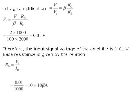
Therefore, the base current of the amplifier is 10 μA.
Question. Two amplifiers are connected one after the other in series (cascaded). The first amplifier has a voltage gain of 10 and the second has a voltage gain of 20. If the input signal is 0.01 volt, calculate the output ac signal.
Answer : Voltage gain of the first amplifier, V1 = 10
Voltage gain of the second amplifier, V2 = 20
Input signal voltage, Vi = 0.01 V
Output AC signal voltage = Vo
The total voltage gain of a two-stage cascaded amplifier is given by the product of voltage gains of both the stages, i.e.,
V = V1 × V2
= 10 × 20 = 200
We have the relation:
V = Vo/Vi
V0 = V × Vi
= 200 × 0.01 = 2 V
Therefore, the output AC signal of the given amplifier is 2 V.
Question. A p-n photodiode is fabricated from a semiconductor with band gap of 2.8 eV. Can it detect a wavelength of 6000 nm?
Answer : Energy band gap of the given photodiode, Eg = 2.8 eV
Wavelength, λ = 6000 nm = 6000 × 10−9 m
The energy of a signal is given by the relation:
E = hc/λ
Where,
h = Planck’s constant
= 6.626 × 10⁻³⁴ Js
c = Speed of light
= 3 × 10⁸ m/s
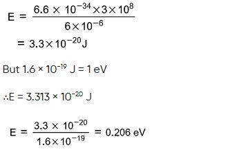
The energy of a signal of wavelength 6000 nm is 0.207 eV, which is less than 2.8 eV − the energy band gap of a photodiode. Hence, the photodiode cannot detect the signal.
Question. The number of silicon atoms per m3 is 5 × 1028. This is doped simultaneously with 5 × 10²² atoms per m3 of Arsenic and 5 × 10²⁰ per m3 atoms of Indium. Calculate the number of electrons and holes. Given that ni= 1.5 × 10¹⁶ m−3. Is the material n-type or p-type?
Answer : Number of silicon atoms, N = 5 × 1028 atoms/m3
Number of arsenic atoms, nAs = 5 × 10²² atoms/m3
Number of indium atoms, nIn = 5 × 10²⁰ atoms/m3
Number of thermally-generated electrons, ni = 1.5 × 10¹⁶ electrons/m3
Number of electrons, ne = 5 × 10²² − 1.5 × 10¹⁶ ≈ 4.99 × 10²²
Number of holes = nh
In thermal equilibrium, the concentrations of electrons and holes in a semiconductor are related as:
nenh = ni2
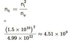
Therefore, the number of electrons is approximately 4.99 × 10²² and the number of holes is about 4.51 × 10⁹. Since the number of electrons is more than the number of holes, the material is an n-type semiconductor.
Question. In an intrinsic semiconductor the energy gap Egis 1.2 eV. Its hole mobility is much smaller than electron mobility and independent of temperature. What is the ratio between conductivity at 600K and that at 300K? Assume that the temperature dependence of intrinsic carrier concentration niis given by
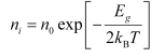
where n0 is a constant.
Answer : Energy gap of the given intrinsic semiconductor, Eg = 1.2 eV
The temperature dependence of the intrinsic carrier-concentration is written as:
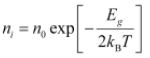
Where,
kB = Boltzmann constant = 8.62 × 10⁻⁵ eV/K
T = Temperature
n0 = Constant
Initial temperature, T1 = 300 K
The intrinsic carrier-concentration at this temperature can be written as:
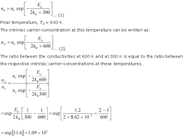
Therefore, the ratio between the conductivities is 1.09 × 10⁵.
Question. In a p-n junction diode, the current I can be expressed as
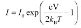
where I0 is called the reverse saturation current, V is the voltage across the diode and is positive for forward bias and negative for reverse bias, and I is the current through the diode, kBis the Boltzmann constant (8.6×10⁻⁵ eV/K) and T is the absolute temperature. If for a given diode I0 = 5 × 10⁻¹² A and T = 300 K, then
(a) What will be the forward current at a forward voltage of 0.6 V?
(b) What will be the increase in the current if the voltage across the diode is increased to 0.7 V?
(c) What is the dynamic resistance?
(d) What will be the current if reverse bias voltage changes from 1 V to 2 V?
Answer : In a p-n junction diode, the expression for current is given as:
Where,
I0 = Reverse saturation current = 5 × 10⁻¹² A
T = Absolute temperature = 300 K
kB = Boltzmann constant = 8.6 × 10⁻⁵ eV/K = 1.376 × 10⁻²³ J K−1
V = Voltage across the diode
(a) Forward voltage, V = 0.6 V

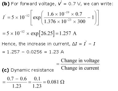
(d) If the reverse bias voltage changes from 1 V to 2 V, then the current (I) will almost remain equal to I0 in both cases. Therefore, the dynamic resistance in the reverse bias will be infinite.
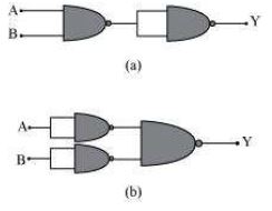
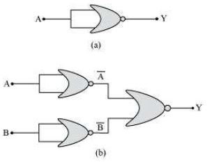
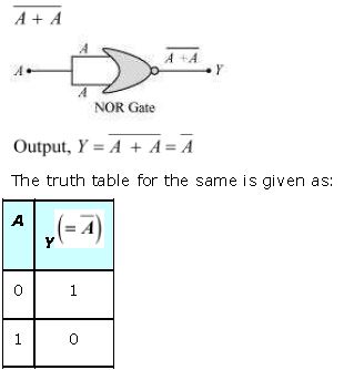
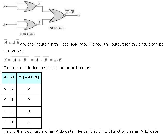
Question. You are given the two circuits as shown in Fig. 14.44. Show that circuit (a) acts as OR gate while the circuit (b) acts as AND gate.
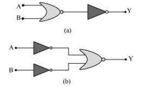
Answer : (a) A and B are the inputs and Y is the output of the given circuit. The left half of the given figure acts as the NOR Gate, while the right half acts as the NOT Gate. This is shown in the following figure.
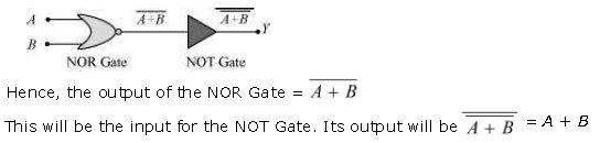
∴Y = A + B
Hence, this circuit functions as an OR Gate.
(b) A and B are the inputs and Y is the output of the given circuit. It can be observed from the following figure that the inputs of the right half NOR Gate are the outputs of the two NOT Gates.

Hence, this circuit functions as an AND Gate.
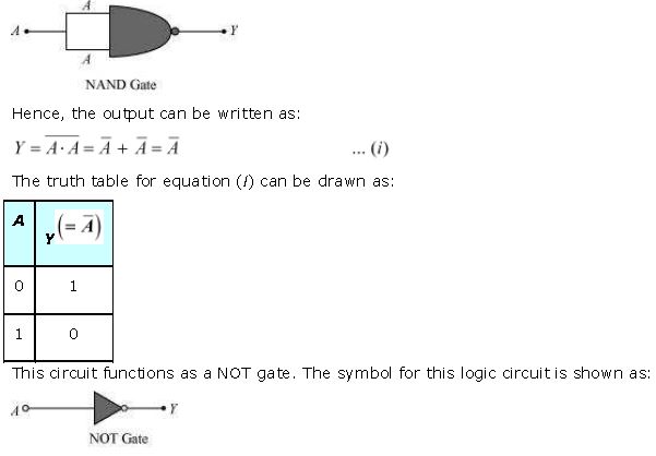
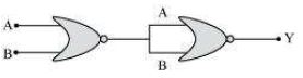
Question. Write the truth table for a NAND gate connected as given in Fig. 14.45.

Hence identify the exact logic operation carried out by this circuit.
Answer : A acts as the two inputs of the NAND gate and Y is the output, as shown in the following figure.
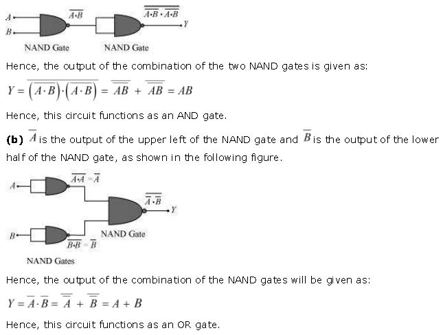
Question. You are given two circuits as shown in Fig. 14.46, which consist of NAND gates. Identify the logic operation carried out by the two circuits.
Answer In both the given circuits, A and B are the inputs and Y is the output.
(a) The output of the left NAND gate will be A¯¯B, as shown in the following figure.
Question. Write the truth table for circuit given in Fig. 14.47 below consisting of NOR gates and identify the logic operation (OR, AND, NOT) which this circuit is performing.
(Hint: A = 0, B = 1 then A and B inputs of second NOR gate will be 0 and hence Y = 1. Similarly work out the values of Y for other combinations of A and B. Compare with the truth table of OR, AND, NOT gates and find the correct one.)
Answer : A and B are the inputs of the given circuit. The output of the first NOR gate is . A ¯+ ¯B It can be observed from the following figure that the inputs of the second NOR gate become the out put of the first one.
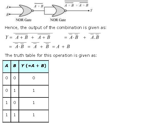
This is the truth table of an OR gate. Hence, this circuit functions as an OR gate.
Question. Write the truth table for the circuits given in Fig. 14.48 consisting of NOR gates only.
Identify the logic operations (OR, AND, NOT) performed by the two circuits.
Answer :
(a) A acts as the two inputs of the NOR gate and Y is the output, as shown in the following figure. Hence, the output of the circuit is
This is the truth table of a NOT gate. Hence, this circuit functions as a NOT gate.
(b) A and B are the inputs and Y is the output of the given circuit. By using the result obtained in solution (a), we can infer that the outputs of the first two NOR gates are A¯ and B¯ as shown in the following figure.
Free study material for Physics
NCERT Solutions Class 12 Physics Chapter 14 Semiconductor Electronics Materials Devices And Simple Circuits
Students can now access the NCERT Solutions for Chapter 14 Semiconductor Electronics Materials Devices And Simple Circuits prepared by teachers on our website. These solutions cover all questions in exercise in your Class 12 Physics textbook. Each answer is updated based on the current academic session as per the latest NCERT syllabus.
Detailed Explanations for Chapter 14 Semiconductor Electronics Materials Devices And Simple Circuits
Our expert teachers have provided step-by-step explanations for all the difficult questions in the Class 12 Physics chapter. Along with the final answers, we have also explained the concept behind it to help you build stronger understanding of each topic. This will be really helpful for Class 12 students who want to understand both theoretical and practical questions. By studying these NCERT Questions and Answers your basic concepts will improve a lot.
Benefits of using Physics Class 12 Solved Papers
Using our Physics solutions regularly students will be able to improve their logical thinking and problem-solving speed. These Class 12 solutions are a guide for self-study and homework assistance. Along with the chapter-wise solutions, you should also refer to our Revision Notes and Sample Papers for Chapter 14 Semiconductor Electronics Materials Devices And Simple Circuits to get a complete preparation experience.
FAQs
The complete and updated is available for free on StudiesToday.com. These solutions for Class 12 Physics are as per latest NCERT curriculum.
Yes, our experts have revised the as per 2026 exam pattern. All textbook exercises have been solved and have added explanation about how the Physics concepts are applied in case-study and assertion-reasoning questions.
Toppers recommend using NCERT language because NCERT marking schemes are strictly based on textbook definitions. Our will help students to get full marks in the theory paper.
Yes, we provide bilingual support for Class 12 Physics. You can access in both English and Hindi medium.
Yes, you can download the entire in printable PDF format for offline study on any device.