

Advanced Study Material for Class 12 Physics: Electronic Devices
Explore structured advanced study materials through the CBSE Class 12 Physics Electronic Devices chapter notes and important questions. Tailored for Class 12 learners, utilizing these Physics resources ensures thorough preparation and strengthens foundational knowledge before final CBSE evaluations.
Practice Class 12 Physics Resources: Electronic Devices
Access the complete useful resource PDF for Class 12 Physics below. Regular practice with these targeted academic notes builds familiarity with complex topics and helps secure higher marks in final school evaluations.
CBSE Class 12 Physics Electronic Devices chapter notes and important questions. Please refer to the examination notes which you can use for preparing and revising for exams. These notes will help you to revise the concepts quickly and get good marks.
ELECTRONIC DEVICES
9. ELECTRONIC DEVICES
GIST
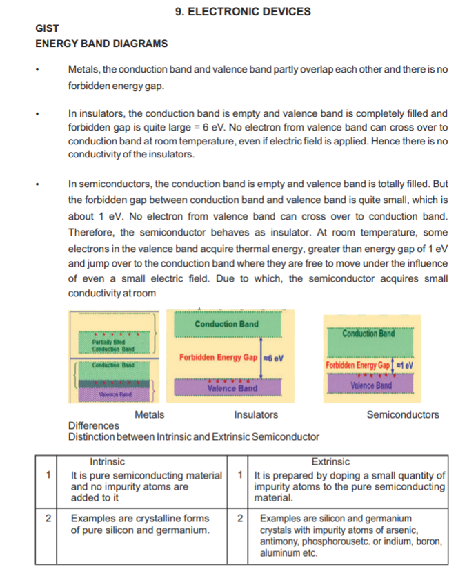
ENERGY BAND DIAGRAMS
- Metals: the conduction band and the valence band partly overlap each other, so there is no forbidden energy gap.
- Insulators: the conduction band is empty and the valence band is completely filled, and the forbidden gap is quite large (about 6 eV). No electron from the valence band can cross over to the conduction band at room temperature, even if an electric field is applied. Hence there is no conductivity of an insulator.
- Semiconductors: the conduction band is empty and the valence band is totally filled, but the forbidden gap between them is quite small, about 1 eV. At 0 K no electron from the valence band can cross over to the conduction band, so the semiconductor behaves as an insulator. At room temperature some electrons in the valence band acquire thermal energy greater than the energy gap of about 1 eV and jump over to the conduction band, where they are free to move under the influence of even a small electric field. Due to this the semiconductor acquires a small conductivity at room temperature.
DISTINCTION BETWEEN INTRINSIC AND EXTRINSIC SEMICONDUCTORS
| Intrinsic semiconductor | Extrinsic semiconductor | |
|---|---|---|
| 1 | It is pure semiconducting material and no impurity atoms are added to it. | It is prepared by doping a small quantity of impurity atoms into the pure semiconducting material. |
| 2 | Examples: crystalline forms of pure silicon and germanium. | Examples: silicon and germanium crystals with impurity atoms of arsenic, antimony, phosphorus etc. or indium, boron, aluminium etc. |
| 3 | The number of free electrons in the conduction band and the number of holes in the valence band are exactly equal and very small indeed. | The number of free electrons and holes is never equal. There is an excess of electrons in n-type semiconductors and an excess of holes in p-type semiconductors. |
| 4 | Its electrical conductivity is low. | Its electrical conductivity is high. |
| 5 | Its electrical conductivity is a function of temperature alone. | Its electrical conductivity depends upon the temperature as well as on the quantity of impurity atoms doped in the structure. |
DISTINCTION BETWEEN n-TYPE AND p-TYPE SEMICONDUCTORS
| n-type semiconductor | p-type semiconductor | |
|---|---|---|
| 1 | It is an extrinsic semiconductor obtained by doping impurity atoms of group V of the periodic table into pure germanium or silicon. | It is an extrinsic semiconductor obtained by doping impurity atoms of group III of the periodic table into pure germanium or silicon. |
| 2 | The impurity atoms added provide extra electrons in the structure and are called donor atoms. | The impurity atoms added create vacancies of electrons (i.e. holes) in the structure and are called acceptor atoms. |
| 3 | Electrons are the majority carriers and holes are the minority carriers. | Holes are the majority carriers and electrons are the minority carriers. |
| 4 | The electron density (\(n_e\)) is much greater than the hole density (\(n_h\)), i.e. \(n_e \gg n_h\). | The hole density (\(n_h\)) is much greater than the electron density (\(n_e\)), i.e. \(n_h \gg n_e\). |
| 5 | The donor energy level is close to the conduction band and far away from the valence band. | The acceptor energy level is close to the valence band and far away from the conduction band. |
| 6 | The Fermi energy level lies between the donor energy level and the conduction band. | The Fermi energy level lies between the acceptor energy level and the valence band. |
p-n JUNCTION
A p-n junction consists of wafers of p-type and n-type semiconductors fused together or grown on each other. At the time of junction formation, free electrons from the n-type semiconductor and holes from the p-type semiconductor diffuse into each other, and their recombination creates a depletion region (a few μm thick). This results in the development of a potential barrier \(V_B\). The potential barrier depends on the material of the semiconductor.
The barrier potential sets up a field across the junction directed from the n-type to the p-type semiconductor. Under the influence of this field, minority charge carriers drift across the junction in a direction opposite to that of the diffusion current, till the two currents equalise and equilibrium is reached. This whole process is complete as soon as the junction is formed.
Depletion region: It is the region near the p-n junction that is depleted of any mobile charge carrier. It consists only of immobile charge carriers. The width of the depletion layer depends on (i) the extent of doping – more doping means a thinner depletion layer; (ii) the type of biasing – forward biasing decreases the thickness of the depletion layer (and reverse biasing increases it).
Potential barrier: The potential difference across the p-n junction under equilibrium is called the potential barrier. It depends on the nature of the semiconductor material.
(a) Diode under equilibrium; (b) barrier potential under no bias (V = 0)
Semiconductor diode: A semiconductor diode is basically a p-n junction with metallic contacts provided at the ends for the application of an external voltage. It is a two-terminal device.
BIASING OF A p-n JUNCTION DIODE
The application of an external voltage to the junction diode in a certain direction is known as biasing of the p-n junction diode. It can be done in two ways: (i) forward biasing and (ii) reverse biasing.
(i) Forward biasing of a p-n junction: A p-n junction is said to be in forward bias when the p region of the diode is maintained at a higher potential with respect to the n region. In forward bias, majority charge carriers in both the regions are pushed through the junction. The depletion region’s width decreases and the junction offers low resistance.
(ii) Reverse biasing of a p-n junction: A p-n junction is said to be in reverse bias when the n region of the diode is maintained at a higher potential with respect to the p region. In reverse bias, majority charge carriers are pushed away from the junction. The depletion region’s width increases. The minority charge carriers are pushed through the junction, thereby causing a small current.
I-V CHARACTERISTICS OF A p-n JUNCTION DIODE
The graphs plotted to show the variation of the current flowing through the junction against the potential difference applied are known as the I-V characteristics of the junction diode.
(a) Forward characteristics of a p-n junction diode
(a) Circuit diagram to draw the forward characteristics
(b) Forward I-V characteristics of a junction diode
In forward bias, the current first increases very slowly, almost negligibly, till the voltage across the diode crosses a threshold value. After the threshold voltage, the diode current increases exponentially. The dynamic resistance of the diode, \(r_d=\dfrac{\Delta V}{\Delta I}\), is small in forward bias.
(b) Reverse characteristics of a p-n junction diode
(a) Circuit diagram to draw the reverse characteristics
(b) Reverse I-V characteristics of a junction diode
In reverse bias, the current is very small (of the order of μA) and almost remains constant with change in bias voltage. It is called the reverse saturation current. However, at a very high reverse bias (the breakdown voltage), the current suddenly increases. In reverse bias, for voltages below the breakdown voltage, the dynamic resistance of the diode is very high.
JUNCTION DIODE AS A RECTIFIER
A rectifier is an electronic circuit which converts a.c. voltage into d.c. voltage. The working of a rectifier is based on the principle that a junction diode allows current to pass only when it is forward biased. Rectifier circuits are basically of two types: (a) half wave rectifier and (b) full wave rectifier.
(a) Half wave rectifier: If an alternating voltage is applied across a diode in series with a load, a pulsating voltage will appear across the load only during the half cycles of the a.c. input during which the diode is forward biased. Such a rectifier circuit, as shown in the figure, is known as a half wave rectifier circuit. The secondary of a transformer supplies the desired a.c. voltage across terminals A and B. When the voltage at A is positive, the diode is forward biased and it conducts. When A is negative, the diode is reverse biased and it does not conduct. Therefore in the positive half cycle of a.c. there is a current through the load resistor \(R_L\) and we get an output voltage, whereas there is no current in the negative half cycle. Thus the output voltage is restricted to only one direction, i.e. it is rectified. Since the rectified output of this circuit is only for half of the input a.c. wave, it is called a half wave rectifier.
Circuit diagram of a half wave rectifier
Input and output waveforms of a half wave rectifier
(b) Full wave rectifier: The circuit using two diodes, as shown in the circuit diagram, gives a rectified output for both the positive and the negative half of the a.c. cycle. Hence it is called a full wave rectifier. In this type of rectifier, each diode rectifies only one half of the a.c. cycle, turn by turn. In one half cycle, diode \(D_1\) conducts, whereas in the next half cycle, diode \(D_2\) conducts, but through the load resistor the current flows for both halves of the a.c. cycle in the same direction. Hence a rectified output is obtained for the full cycle of the input a.c. voltage.
Circuit diagram for a full wave rectifier (centre-tap transformer)
Input and output waveforms for a full wave rectifier
ZENER DIODE
A Zener diode is a special purpose junction diode designed to operate under reverse bias in the reverse breakdown region. It is used as a voltage regulator for the output of rectifiers. It is a heavily doped p-n junction having a very thin depletion layer, so the electric field across it is very high (of the order of \(10^6\) V/m). When a small reverse bias voltage is applied across the Zener diode junction, the field increases very rapidly, causing internal field emission and hence a reverse breakdown at a relatively low voltage. The reverse bias current (known as the Zener current) increases abruptly for a negligible increase in reverse bias voltage in the breakdown region, as shown below.
Symbol of Zener diode
I-V characteristics of Zener diode
Zener diode as a voltage regulator: A Zener diode is used to stabilise the output voltage of a rectifier by absorbing the fluctuations of the rectified output voltage. The unregulated d.c. voltage (the filtered output of a rectifier) is connected to the Zener diode through a series resistance \(R_s\) such that the Zener diode is reverse biased. If the input voltage increases, the current through \(R_s\) and the Zener diode also increases. This increases the voltage drop across \(R_s\) without any change in the voltage across the Zener diode. This is because in the breakdown region, the Zener voltage remains constant even though the current through the Zener diode changes. Similarly, if the input voltage decreases, the current through \(R_s\) and the Zener diode also decreases. The voltage drop across \(R_s\) decreases without any change in the voltage across the Zener diode. Thus any increase or decrease in the input voltage results in an increase or decrease of the voltage drop across \(R_s\), without any change in the voltage across the Zener diode. Thus the Zener diode acts as a voltage regulator.
OPTOELECTRONIC JUNCTION DEVICES
The semiconductor diodes in which the charge carriers are generated by photons are known as optoelectronic devices. They are the photodiode, the LED and the solar cell.
(i) Photodiode: It is used for detecting optical signals. A photodiode is a p-n junction diode fabricated with a transparent window to allow light to fall on the diode. It is operated under reverse bias. When the photodiode is illuminated with light (photons) with energy (\(h\nu\)) greater than the energy gap (\(E_g\)) of the semiconductor, then electron-hole pairs are generated due to the absorption of photons. The diode is fabricated such that the generation of e-h pairs takes place in or near the depletion region of the diode. Due to the electric field of the junction, electrons and holes are separated before they recombine. The direction of the electric field is such that electrons reach the n-side and holes reach the p-side. Electrons are collected on the n-side and holes are collected on the p-side, giving rise to an emf. When an external load is connected, current flows. The magnitude of the photocurrent depends on the intensity of the incident light (photocurrent is directly proportional to the intensity of the incident light).
Reverse I-V characteristics of a photodiode: the reverse current increases with the intensity of light
(ii) Light Emitting Diode (LED): It is a heavily doped p-n junction which, under forward bias, emits spontaneous radiation. The diode is encapsulated with a transparent cover so that the emitted light can come out. When the diode is forward biased, electrons are sent from n → p (where they are minority carriers) and holes are sent from p → n (where they are minority carriers). At the junction boundary the concentration of minority carriers increases compared to the equilibrium concentration (i.e. when there is no bias). Thus at the junction boundary, on either side of the junction, excess minority carriers are present, which recombine with majority carriers near the junction. On recombination, the energy is released in the form of photons. Photons with energy equal to or slightly less than the band gap are emitted.
(a) Biasing of LED
(b) I-V characteristics of LED
- The intensity of the emitted light depends on the forward current flowing through the LED. When the forward current of the diode is small, the intensity of the light emitted is small. As the forward current increases, the intensity of light increases and reaches a maximum.
- The colour of the light emitted by an LED depends on the composition of the material of the LED (wavelength of emitted light \(\lambda=\dfrac{hc}{E_g}\)).
LEDs have the following advantages over conventional incandescent low power lamps:
- Low operational voltage and less power.
- Fast action and no warm-up time required.
- The bandwidth of the emitted light is 100 Å to 500 Å, or in other words it is nearly (but not exactly) monochromatic.
- Long life and ruggedness.
- Fast on-off switching capability.
(iii) Solar cell: A solar cell is basically a p-n junction which generates an emf when solar radiation falls on the p-n junction. It is very lightly doped, in which the depletion layer is very wide, and the n and p regions are very thin. The generation of emf by a solar cell, when light falls on it, is due to the following three basic processes: generation, separation and collection.
- generation of e-h pairs due to light (with \(h\nu > E_g\)) close to the junction;
- separation of electrons and holes due to the electric field of the depletion region. Electrons are swept to the n-side and holes to the p-side;
- the electrons reaching the n-side are collected by the front contact and the holes reaching the p-side are collected by the back contact. Thus the p-side becomes positive and the n-side becomes negative, giving rise to a photovoltage.
When an external load is connected as shown in the figure, a photocurrent \(I_L\) flows through the load. A typical I-V characteristic of a solar cell is drawn in the fourth quadrant.
(a)
(b)
JUNCTION TRANSISTOR
A transistor has three doped regions forming two p-n junctions between them. There are two types of transistor:
- n-p-n transistor: Here two segments of n-type semiconductor (emitter and collector) are separated by a segment of p-type semiconductor (base).
- p-n-p transistor: Here two segments of p-type semiconductor (termed emitter and collector) are separated by a segment of n-type semiconductor (termed base).
- Emitter: This is the segment on one side of the transistor. It is of moderate size and heavily doped. It supplies a large number of majority carriers for the current flow through the transistor.
- Base: This is the central segment. It is very thin and lightly doped.
- Collector: This segment collects a major portion of the majority carriers supplied by the emitter. The collector side is moderately doped and larger in size as compared to the emitter.
Transistor action (p-n-p transistor): The emitter-base junction of the transistor is forward biased, whereas the collector-base junction is reverse biased, in its active state. The heavily doped emitter has a high concentration of majority carriers. These majority carriers enter the base region in large numbers. The base is thin and lightly doped, so the majority carriers there are few. In a p-n-p transistor the majority carriers in the base are electrons, since the base is of n-type semiconductor. The large number of holes entering the base from the emitter swamps the small number of electrons there. As the base-collector junction is reverse biased, these holes, which appear as minority carriers at the junction, can easily cross the junction and enter the collector. The holes in the base could move either towards the base terminal to combine with the electrons entering from outside, or cross the junction to enter the collector and reach the collector terminal. The base is made thin so that most of the holes find themselves near the reverse-biased base-collector junction and so cross the junction instead of moving to the base terminal. The current entering the emitter from outside is equal to the emitter current \(I_E\). Similarly the current emerging from the base terminal is \(I_B\) and that from the collector terminal is \(I_C\). It is obvious from the above description that the emitter current is the sum of the collector current and the base current:
\[I_E = I_C + I_B\]
COMMON EMITTER TRANSISTOR CHARACTERISTICS
Input characteristics: the plot of base current \(I_B\) versus base-emitter voltage \(V_{BE}\) at a fixed collector-emitter voltage \(V_{CE}\). Output characteristics: the plot of collector current \(I_C\) versus collector-emitter voltage \(V_{CE}\) for different fixed values of \(I_B\).
Circuit diagram to draw the n-p-n transistor characteristics in CE configuration
Input characteristic
Output characteristics
The input characteristic of a transistor is identical for different output voltages. These characteristics are like the forward characteristics of a junction diode.
The output characteristics show that when \(I_B\) increases, \(I_C\) also increases. The plot of \(I_C\) versus \(V_{CE}\) for different fixed values of \(I_B\) gives one output characteristic, so there will be different output characteristics corresponding to different values of \(I_B\), as shown.
Saturation state: The output characteristics show that initially, for very small values of \(V_{CE}\), \(I_C\) increases almost linearly. This happens because the base-collector junction is not reverse biased and the transistor is not in the active state. In fact, the transistor is in the saturation state and the current is controlled by the supply voltage \(V_{CC}\) (\(=V_{CE}\)) in this part of the characteristic.
Active state: When \(V_{CE}\) is more than that required to reverse bias the base-collector junction, \(I_C\) increases very little with \(V_{CE}\). The reciprocal of the slope of the linear part of the output characteristic gives the value of the output resistance \(r_o\). The output resistance of the transistor is mainly controlled by the bias of the base-collector junction. The high magnitude of the output resistance (of the order of 100 kΩ) is due to the reverse-biased state of this diode. In this state, for a small change in base current, a large change is observed in collector current.
Output resistance and current gain (amplification factor):
\[r_o=\left(\frac{\Delta V_{CE}}{\Delta I_C}\right)_{I_B=\text{constant}},\qquad \beta=\left(\frac{\Delta I_C}{\Delta I_B}\right)_{V_{CE}=\text{constant}}\]
Cut-off state: When the base-emitter voltage is negligible such that \(I_B=0\), then \(I_C\) is almost zero. This state of the transistor is said to be the cut-off state.
TRANSISTOR AS AN AMPLIFIER IN COMMON EMITTER CONFIGURATION
An amplifier is an electronic circuit that increases the amplitude of the a.c. voltage using d.c. energy. For using the transistor as an amplifier we use the active region of the \(V_o\) versus \(V_i\) curve.
Phase reversal: The slope of the linear part of the curve represents the rate of change of the output with the input. It is negative because the output is \(V_{CC}-I_CR_L\). That is why, as the input voltage of the CE amplifier increases, its output voltage decreases, and the output is said to be out of phase with the input.
Voltage amplification by the amplifier is defined as \(A_v=\Delta V_o/\Delta V_i\), where \(\Delta V_o\) and \(\Delta V_i\) are small changes in the output and input voltages. If the \(V_{BB}\) voltage has a fixed value corresponding to the mid-point of the active region, the circuit will behave as a CE amplifier.
If we first assume \(v_i=0\), then applying Kirchhoff’s law to the output and input loops,
\[V_{CC}=V_{CE}+I_CR_L\quad\text{and}\quad V_{BB}=V_{BE}+I_BR_B\]
When \(v_i\) is not zero we get
\[V_i+V_{BB}=V_{BE}+I_BR_B+\Delta V_{BE}+\Delta I_BR_B\]
If the input junction resistance is \(R_i=\dfrac{\Delta V_{BE}}{\Delta I_B}\), the change in \(I_B\) causes a change in \(I_C\):
\[\beta_{ac}=\frac{\Delta I_C}{\Delta I_B}=\frac{i_c}{i_b}\]
which is also known as the a.c. current gain. The change in \(I_C\) due to a change in \(I_B\) causes a change in \(V_{CE}\) and the voltage drop across the resistor \(R_L\), because \(V_{CC}\) is fixed:
\[\Delta V_{CC}=\Delta V_{CE}+R_L\Delta I_C=0\]
\[\text{or}\quad \Delta V_{CE}=-R_L\Delta I_C\]
The change in \(V_{CE}\) is the output voltage \(v_o\):
\[v_o=\Delta V_{CE}=-\beta_{ac}R_L\Delta I_B\]
The voltage gain of the amplifier is
\[A_v=\frac{v_o}{v_i}=\frac{\Delta V_{CE}}{r\,\Delta I_B}=-\frac{\beta_{ac}R_L}{r}\]
ANALOGUE AND DIGITAL SIGNALS
A signal in the form of continuous, time-varying voltage or current is called an analogue signal. A pulse waveform in which only discrete values of voltage or current are possible is called a digital signal.
LOGIC GATES
A logic gate is a digital circuit that follows a certain logical relationship between one or more than one input and the output; the voltages are always in two states only. The basic logic gates are:
OR gate: The output of an OR gate is 1 if at least one of the inputs is at the 1 state.
AND gate: The output of an AND gate is 1 only when all the inputs are at the 1 state.
NOT gate: It is a one-input gate. The output of a NOT gate is the inverse of the input.
Apart from the above basic gates, there are two universal gates:
NOR gate: The output of a NOR gate is 0 if at least one of the inputs is at the 1 state.
NAND gate: The output of a NAND gate is 0 only when all the inputs are at the 1 state.
QUESTIONS
SEMICONDUCTORS
What is the order of the energy gap in an intrinsic semiconductor?
Answer: About 1 eV (silicon ≈ 1.1 eV, germanium ≈ 0.7 eV).
How does the energy gap vary in a semiconductor when doped with a penta-valent element?
Answer: The effective energy gap decreases. A penta-valent (donor) impurity creates a donor energy level just below the conduction band, so electrons need much less energy to reach the conduction band.
How does the conductivity change with temperature in a semiconductor?
Answer: The conductivity increases as the temperature rises. More electrons gain enough thermal energy to jump to the conduction band, so more electron-hole pairs are formed.
What type of semiconductor do we get when Ge is doped with indium? When Si is doped with bismuth?
Answer: Ge doped with indium (trivalent) gives a p-type semiconductor. Si doped with bismuth (pentavalent) gives an n-type semiconductor.
In a semiconductor the concentration of electrons is \(8\times10^{13}\ \text{cm}^{-3}\) and of holes is \(5\times10^{12}\ \text{cm}^{-3}\). Is it a p-type or an n-type semiconductor?
Answer: n-type, because the electron concentration is much greater than the hole concentration (\(n_e > n_h\)).
Draw the energy band diagram of a p-type semiconductor.
Answer: See the figure: an acceptor level \(E_A\) lies just above the top of the valence band.
What is the Fermi energy level?
Answer: It is the energy level at which the probability of finding an electron is ½ (at temperatures above 0 K); at 0 K it is the highest energy level occupied by electrons. In an intrinsic semiconductor it lies in the middle of the forbidden gap.
The energy gaps of a conductor, a semiconductor and an insulator are \(E_1, E_2, E_3\) respectively. Arrange them in increasing order.
Answer: \(E_1 < E_2 < E_3\) (conductor < semiconductor < insulator).
Name the factor that determines whether an element is a conductor or a semiconductor.
Answer: The energy gap (forbidden gap) between the valence band and the conduction band. For a conductor there is no gap (the bands overlap); for a semiconductor it is small, about 1 eV.
Why are semiconductors opaque to visible light but transparent to infrared radiation?
Answer: The photons of infrared radiation have smaller energies, so they fall short of exciting the electrons in the valence band. Hence infrared radiation passes through the semiconductor as such, i.e. a semiconductor is transparent to infrared radiation.
The ratio of the number of free electrons to holes, \(n_e/n_h\), is 1 for material A and less than 1 for material B. Name the type of semiconductor to which A and B belong.
Answer: If \(n_e/n_h=1\), A is an intrinsic semiconductor. If \(n_e/n_h<1\), i.e. \(n_e<n_h\), B is a p-type semiconductor.
A semiconductor has equal electron and hole concentrations of \(6\times10^{8}\ \text{m}^{-3}\). On doping with a certain impurity, the electron concentration increases to \(9\times10^{12}\ \text{m}^{-3}\). (i) Identify the new semiconductor obtained after doping. (ii) Calculate the new hole concentration.
Answer: (i) n-type semiconductor. (ii) \(n_h = 4\times10^{4}\ \text{m}^{-3}\).
Using \(n_en_h=n_i^2\):
\[n_h=\frac{n_i^2}{n_e}=\frac{6\times10^{8}\times6\times10^{8}}{9\times10^{12}}=4\times10^{4}\ \text{m}^{-3}\]
p-n JUNCTION DIODE
How does the width of the depletion layer change in reverse bias of a p-n junction diode?
Answer: It increases, because the majority carriers are pushed away from the junction.
Draw the V-I characteristic graph for a Zener diode.
Answer: See the figure.
In the given diagram, is the diode reverse or forward biased?
Answer: Forward biased.
The p-side (anode) of the diode is connected, through R, to the +10 V point and the n-side (cathode) is connected to earth (0 V), so the p-side is at the higher potential.
Why is a photodiode usually operated in reverse bias?
Answer: In reverse bias the current in the dark is very small, so the extra current produced when light falls on the diode (the new electron-hole pairs) is a large fraction of the total and is easy to measure. In forward bias the current is already large and the change due to light would be a negligible fraction of it.
State the factors which control the wavelength and the intensity of the light emitted by an LED.
Answer: (i) The nature (material) of the semiconductor controls the wavelength (colour) of the light emitted. (ii) The forward current controls the intensity of the light emitted.
With the help of a diagram show the biasing of a light emitting diode. Give two advantages over a conventional incandescent lamp.
Answer: Advantages: (i) it is monochromatic (nearly one colour); (ii) it consumes less power (low operating voltage). The LED is forward biased, as in the figure.
Draw a circuit diagram to show how a photodiode is biased.
Answer: A photodiode is reverse biased, as shown.
Pure Si at 300 K has equal electron and hole concentrations of \(1.5\times10^{16}\ \text{per m}^3\). Doping by indium increases the hole concentration to \(4.5\times10^{22}\ \text{per m}^3\). Calculate the new electron concentration.
Answer: \(n_e = 5\times10^{9}\ \text{m}^{-3}\).
Using \(n_en_h=n_i^2\):
\[n_e=\frac{n_i^2}{n_h}=\frac{(1.5\times10^{16})^2}{4.5\times10^{22}}=5\times10^{9}\ \text{m}^{-3}\]
In the following diagram, identify the diodes which are forward biased and which are reverse biased.
Answer: (i) reverse biased; (ii) forward biased; (iii) reverse biased; (iv) forward biased.
A diode is forward biased when its p-side (the triangle’s flat side) is at a higher potential than its n-side (the bar side). In (i) the p-side is at 0 V and the n-side is at +5 V. In (ii) the p-side is at +10 V and the n-side is at +5 V. In (iii) the p-side is at −10 V and the n-side is at 0 V. In (iv) the p-side is at −5 V and the n-side is at −12 V.
Determine the current through the resistance R in each circuit. The diodes \(D_1\) and \(D_2\) are identical and ideal.
Answer: (i) \(I\approx0.19\) A; (ii) no current flows.
In circuit (i) both \(D_1\) and \(D_2\) are forward biased, hence both conduct and the resistance of each diode is 0. Therefore:
\[I=\frac{3}{16}\approx0.19\ \text{A}\]
In circuit (ii) diode \(D_1\) is forward biased and \(D_2\) is reverse biased, therefore the resistance of \(D_1\) is 0 and the resistance of \(D_2\) is infinite. Hence \(D_1\) conducts and \(D_2\) does not conduct. No current flows in the circuit.
(i)
(ii)
From the given graph identify the knee voltage and the breakdown voltage. Explain.
Answer: The knee voltage is on the forward side and the breakdown voltage is on the reverse side of the graph.
Knee voltage: the forward bias voltage beyond which the forward current starts to rise sharply (about 0.7 V for silicon and 0.3 V for germanium). Breakdown voltage: the reverse bias voltage at which the reverse current suddenly increases to a large value.
Which special type of diode acts as a voltage regulator? Give its symbol. Draw its V-I characteristics.
Answer: The Zener diode. It is operated in reverse bias in the breakdown region, where the voltage across it stays almost constant while the current changes widely.
TRANSISTORS
How does the d.c. current gain of a transistor change when the width of the base region is increased?
Answer: It decreases, because more charge carriers recombine in the wider base before reaching the collector.
In only one of the circuits given below does the lamp “L” glow. Identify the circuit. Give a reason for your answer.
Answer: Circuit (II).
In circuit (I) the base is joined to the emitter through R, so the emitter-base junction has no source of emf across it. Therefore \(I_C=0\) and the bulb will not glow.
In circuit (II) the emitter-base junction is forward biased; therefore the lamp “L” will glow.
In circuit (III) the emitter-base junction is reverse biased, so the bulb will not glow.
Why do we prefer an n-p-n transistor to a p-n-p transistor for faster action?
Answer: In an n-p-n transistor the current conduction is mainly by free electrons, whereas in a p-n-p transistor it is mainly by holes. The mobility of electrons is greater than that of holes, so the n-p-n transistor acts faster.
In which mode (cut-off, active or saturation) is the transistor used as a switch? Why?
Answer: In the cut-off and saturation modes.
In cut-off (\(I_C\approx0\)) the transistor behaves like an open switch (OFF), and in saturation (\(V_{CE}\approx0\), large \(I_C\)) it behaves like a closed switch (ON).
In an n-p-n transistor circuit, the collector current is 5 mA. If 95% of the electrons emitted reach the collector region, what is the base current?
Answer: \(I_B\approx0.26\) mA.
\[I_C=95\%\text{ of }I_E=\frac{95}{100}I_E\ \Rightarrow\ I_E=\frac{100}{95}\times5=5.26\ \text{mA}\]
\[I_E=I_C+I_B\ \Rightarrow\ I_B=5.26-5=0.26\ \text{mA}\]
Which of the input and output circuits of a transistor has the higher resistance, and why?
Answer: The output circuit has the higher resistance.
The output (collector-base) junction is reverse biased, so its resistance \(r_o\) is very high (of the order of 100 kΩ), whereas the input (emitter-base) junction is forward biased and has a low resistance \(r_i\). Thus \(r_o\gg r_i\) (the resistance of the output circuit is \(10^4\) times that of the input circuit, i.e. \(r_o=10^4\,r_i\)).
The base current of a transistor is 105 μA and the collector current is 2.05 mA. (a) Determine the value of \(\beta\) and \(I_e\). (b) A change of 27 μA in the base current produces a change of 0.65 mA in the collector current. Find \(\beta_{ac}\).
Answer: (a) \(\beta\approx19.5\), \(I_e=2.155\) mA; (b) \(\beta_{ac}\approx24.1\).
\[\beta=\frac{I_C}{I_B}=\frac{2.05\times10^{-3}}{105\times10^{-6}}=19.5\]
\[I_E=I_B+I_C=2.155\times10^{-3}\ \text{A}\]
\[\beta_{ac}=\frac{\Delta I_C}{\Delta I_B}=\frac{0.65\times10^{-3}}{27\times10^{-6}}=24.1\]
Explain, through a labelled circuit diagram, the working of a transistor as an amplifier in common emitter configuration. Obtain the expressions for current gain, voltage gain and power gain.
Answer: See the circuit below and the working that follows.
The emitter-base junction is forward biased by \(V_{BB}\) and the collector-base junction is reverse biased by \(V_{CC}\), so the transistor works in the active region. A small a.c. signal \(v_i\) in the base circuit produces a small change \(\Delta I_B\) in the base current, which produces a much larger change \(\Delta I_C\) in the collector current. This change develops a larger a.c. voltage across the load resistor \(R_L\).
Current gain:
\[\beta_{ac}=\left(\frac{\Delta I_C}{\Delta I_B}\right)_{V_{CE}}\]
Voltage gain: since \(V_{CC}=V_{CE}+I_CR_L\), \(\Delta V_{CE}=-R_L\Delta I_C\), and with input resistance \(r_i=\Delta V_{BE}/\Delta I_B\):
\[A_v=\frac{\Delta V_{CE}}{\Delta V_{BE}}=-\frac{R_L\Delta I_C}{r_i\Delta I_B}=-\beta_{ac}\frac{R_L}{r_i}\]
Power gain: power gain = current gain × voltage gain, so in magnitude
\[A_p=\beta_{ac}\times|A_v|=\beta_{ac}^2\frac{R_L}{r_i}\]
Draw a circuit diagram to study the input and output characteristics of an n-p-n transistor in common emitter configuration. Draw the graphs for the input and output characteristics.
Answer: The circuit and the graphs are shown below.
Define the trans-conductance of a transistor.
Answer: The trans-conductance is the ratio of the small change in collector current to the small change in base-emitter voltage, at constant collector-emitter voltage:
\[g_m=\frac{\Delta I_C}{\Delta V_{BE}}\]
How does the collector current change in a junction transistor if the base region has a larger width?
Answer: The collector current decreases.
The input resistance of a common emitter amplifier is 2 kΩ. The current gain is 20. If the load resistance is 5 kΩ, calculate the trans-conductance and the voltage gain.
Answer: \(g_m=0.01\) S (10 mS); \(A_v=50\) (in magnitude).
\[g_m=\frac{\beta}{R_i}=\frac{20}{2000}=0.01\ \text{S}\]
\[A_v=\beta\frac{R_L}{R_i}=20\times\frac{5}{2}=50\]
Define input resistance, output resistance, current amplification factor and voltage amplification factor for a common emitter configuration of a transistor.
Answer: All are defined for small changes:
Input resistance: \(r_i=\left(\dfrac{\Delta V_{BE}}{\Delta I_B}\right)_{V_{CE}}\).
Output resistance: \(r_o=\left(\dfrac{\Delta V_{CE}}{\Delta I_C}\right)_{I_B}\).
Current amplification factor: \(\beta=\left(\dfrac{\Delta I_C}{\Delta I_B}\right)_{V_{CE}}\).
Voltage amplification factor: \(A_v=\dfrac{\Delta V_o}{\Delta V_i}=-\beta_{ac}\dfrac{R_L}{r_i}\).
A change of 0.2 mA in the base current causes a change of 5 mA in the collector current in a common emitter amplifier. (i) Find the a.c. current gain of the transistor. (ii) If the input resistance is 2 kΩ and the voltage gain is 75, calculate the load resistance used in the circuit.
Answer: (i) \(\beta_{ac}=25\); (ii) \(R_L=6\ \text{k}\Omega\).
\[\beta_{ac}=\frac{\Delta I_C}{\Delta I_B}=\frac{5}{0.2}=25\]
\[A_v=\beta_{ac}\frac{R_L}{R_i}\ \Rightarrow\ R_L=\frac{A_vR_i}{\beta_{ac}}=\frac{75\times2}{25}=6\ \text{k}\Omega\]
In a transistor the base current is changed by 20 μA. This results in a change of 0.02 V in the base-emitter voltage and a change of 2 mA in the collector current. Find (i) the input resistance, (ii) the trans-conductance.
Answer: (i) \(R_i=1\ \text{k}\Omega\); (ii) \(g_m=0.1\) S.
\[R_i=\frac{\Delta V_{BE}}{\Delta I_B}=\frac{0.02}{20\times10^{-6}}=1000\ \Omega\]
\[g_m=\frac{\Delta I_C}{\Delta V_{BE}}=\frac{2\times10^{-3}}{0.02}=0.1\ \text{S}\]
With the help of a circuit diagram, explain the action of a transistor.
Answer: Action of a p-n-p transistor (an n-p-n transistor works in the same way, with the roles of electrons and holes interchanged):
The emitter-base junction is forward biased (by \(V_{EE}\)) and the collector-base junction is reverse biased (by \(V_{CC}\)). The heavily doped emitter sends a large number of holes into the thin, lightly doped base. A very small number of these combine with the few electrons in the base (giving the small base current \(I_B\)); the rest, being minority carriers in the base, are swept across the reverse-biased base-collector junction into the collector (giving \(I_C\)). Hence
\[I_E=I_C+I_B\]
Draw the transfer characteristics of a transistor in common emitter configuration. Explain briefly the meaning of the terms active region and cut-off region in this characteristic.
Answer: The transfer characteristic is the plot of the output voltage \(V_o\) against the input voltage \(V_i\).
Cut-off region: the base-emitter voltage is too small for the emitter junction to conduct, so \(I_B=0\), \(I_C\approx0\) and \(V_o\) stays at \(V_{CC}\). Active region: the emitter-base junction is forward biased and the collector-base junction is reverse biased; here \(V_o\) falls almost linearly as \(V_i\) increases, and the transistor works as an amplifier. In the saturation region \(V_o\) is small and nearly constant.
Explain, with the help of a circuit diagram, the working of an n-p-n transistor as a common emitter amplifier. Draw the input and output waveforms.
Answer: The circuit is shown below.
With \(V_{BB}\) fixed at the mid-point of the active region, the input signal \(v_i\) changes the base current. The collector current changes \(\beta\) times as much, and since \(V_{CE}=V_{CC}-I_CR_L\), the output voltage rises when the input falls and vice versa. The output is therefore an amplified signal which is out of phase (180°) with the input.
Draw a labelled circuit diagram of a common emitter amplifier using a p-n-p transistor. Define the voltage gain and write its expression. Explain how the input and output voltages are out of phase by 180° for a common emitter transistor amplifier.
Answer: The circuit is shown below.
Voltage gain is the ratio of the small change in output voltage to the small change in input voltage:
\[A_v=\frac{\Delta V_o}{\Delta V_i}=-\beta_{ac}\frac{R_L}{r_i}\]
Phase difference: \(V_{CC}=V_{CE}+I_CR_L\) with \(V_{CC}\) fixed, so \(\Delta V_{CE}=-R_L\Delta I_C\). When the input voltage increases, \(I_B\) and therefore \(I_C\) increase, the drop across \(R_L\) increases and \(V_{CE}\) (the output) decreases. The output voltage thus changes in the opposite sense to the input, i.e. it is 180° out of phase with the input.
LOGIC GATES
Modern technology uses poly-silicon instead of metal to form the gate. Why?
Answer: Poly-silicon can withstand the high temperatures used in the later steps of fabrication (which a metal gate cannot), and it allows the gate to be self-aligned with the source and drain.
Identify the logic gate. Give its truth table and the output waveform.
Answer: NAND gate.
The circuit is an AND gate followed by a NAND gate whose two inputs are joined together (so it acts as a NOT gate). Hence \(Y=\overline{A\cdot B}\).
| A | B | Y |
|---|---|---|
| 0 | 0 | 1 |
| 0 | 1 | 1 |
| 1 | 0 | 1 |
| 1 | 1 | 0 |
Draw the logic circuit and the output waveform for the given output Y = 0, 0, 1, 1.
Answer: The output of the AND gate is \(Y=A\cdot B\); consequently the inputs of the OR gate are \(A\) and \(A\cdot B\). Then the final output is \(Y'=A+A\cdot B\).
| A | B | Y = A·B | Y′ = A + Y |
|---|---|---|---|
| 0 | 0 | 0 | 0 |
| 0 | 1 | 0 | 0 |
| 1 | 0 | 0 | 1 |
| 1 | 1 | 1 | 1 |
Construct the truth table for the Boolean equation \(Y'=(A+B)\cdot C\) and represent it by a logic circuit.
Answer: The output of the OR gate is \(A+B\). Consequently the inputs of the AND gate are \(A+B\) and \(C\), and the Boolean equation for the given circuit is \(Y'=(A+B)C=Y\cdot C\), where \(Y=A+B\).
| A | B | C | Y = A + B | Y′ = (A + B)·C = Y·C |
|---|---|---|---|---|
| 0 | 0 | 0 | 0 | 0 |
| 0 | 0 | 1 | 0 | 0 |
| 0 | 1 | 0 | 1 | 0 |
| 0 | 1 | 1 | 1 | 1 |
| 1 | 0 | 0 | 1 | 0 |
| 1 | 0 | 1 | 1 | 1 |
| 1 | 1 | 0 | 1 | 0 |
| 1 | 1 | 1 | 1 | 1 |
Construct an AND gate using NAND gates and give its truth table.
Answer: An AND gate is obtained by joining the output of a NAND gate to both inputs of a second NAND gate (used as a NOT gate):
| A | B | Y = A·B |
|---|---|---|
| 0 | 0 | 0 |
| 0 | 1 | 0 |
| 1 | 0 | 0 |
| 1 | 1 | 1 |
Identify which basic gate (OR, AND or NOT) is represented by the circuits in the dotted-line boxes 1, 2 and 3. Give the truth table for the entire circuit for all possible values of A and B.
Answer: The dotted-line box 1 represents a NOT gate. The dotted-line box 2 represents an OR gate (here we use De Morgan’s theorem). The dotted-line box 3 represents an AND gate.
The output of box 1 is \(\bar A\); box 2 gives \(\bar A+B\); box 3 then gives \(Y=(\bar A+B)\cdot B=B\).
| A | B | Output of box 1 (Ā) | Output of box 2 (Ā + B) | Y = (Ā + B)·B |
|---|---|---|---|---|
| 0 | 0 | 1 | 1 | 0 |
| 0 | 1 | 1 | 1 | 1 |
| 1 | 0 | 0 | 0 | 0 |
| 1 | 1 | 0 | 1 | 1 |
Two input waveforms A and B, shown in figure (a), are applied to an AND gate. Write the output.
Answer: The output \(Y=A\cdot B\) is 1 only in the time interval in which both A and B are 1.
| Time interval | 1 | 2 | 3 | 4 | 5 | 6 |
|---|---|---|---|---|---|---|
| Input A | 0 | 1 | 1 | 0 | 0 | 1 |
| Input B | 0 | 0 | 1 | 1 | 0 | 0 |
| Output Y = A·B | 0 | 0 | 1 | 0 | 0 | 0 |
A circuit symbol of a logic gate and two input waveforms A and B are shown. (a) Name the logic gate. (b) Give the output waveform.
Answer: (a) AND gate. (b) The output Y is high only while both A and B are high; otherwise it is low.
Current amplifier \(=\Delta I_c/\Delta I_b=(9.5-2.5)/(50\times10^{-6})\)
Identify the logic gate.
Answer: OR gate.
Each input is first inverted by a NOT gate and the results are fed to a NAND gate, so \(Y=\overline{\bar A\cdot\bar B}=A+B\), which is an OR gate.
Identify the logic gates.
Answer: P is an OR gate, Q is an AND gate and R is a NAND gate.
Identify the gate.
Answer: AND gate.
Each input is inverted by a NOT gate and the results are fed to a NOR gate, so \(Y=\overline{\bar A+\bar B}=A\cdot B\), which is an AND gate.
Free study material for Physics
Physics Class 12 Exam Resources: Electronic Devices
Core Study Kit: Class 12 Physics Electronic Devices
Explore essential learning tools for Class 12 Physics Electronic Devices. This curated collection features in-depth notes and targeted practice questions built around the active 2026 curriculum to streamline your daily revision.
NCERT-Aligned Solutions for Electronic Devices
Built using official NCERT guidelines for Class 12 Physics, these materials provide reliable academic support. Integrating past examination questions and step-by-step solutions helps students understand official CBSE grading criteria.
Next Steps in Your Exam Preparation
Wrap up your chapter revision by testing your knowledge against standard objective question formats. Explore our full library of free, up-to-date sample papers and online assessments to secure top grades in your CBSE examinations.
FAQs
Our advanced study package for Electronic Devices includes detailed concepts, diagrams, Mind Maps, and explanation of complex topics to ensure Class 12 students learn as per syllabus for 2026 exams.
The Mind Maps provided for Electronic Devices act as visual anchors which will help faster recall during high-pressure exams.
Yes, teachers use our Class 12 Physics resources for lesson planning as they are in simple language and have lot of solved examples.
Yes, You can download the complete, mobile-friendly PDF of the Physics Electronic Devices advanced resources for free.
Yes, our subject matter experts have updated the Electronic Devices material to align with the rationalized NCERT textbooks and have removed deleted topics and added new competency-based questions.