
Read and download the CBSE Class 12 Physics Semiconductor Assignment for the 2026-27 academic session. We have provided comprehensive Class 12 Physics school assignments that have important solved questions and answers for Chapter 14 Semiconductor Electronics Materials Devices And Simple Circuits. These resources have been carefuly prepared by expert teachers as per the latest NCERT, CBSE, and KVS syllabus guidelines.
Solved Assignment for Class 12 Physics Chapter 14 Semiconductor Electronics Materials Devices And Simple Circuits
Practicing these Class 12 Physics problems daily is must to improve your conceptual understanding and score better marks in school examinations. These printable assignments are a perfect assessment tool for Chapter 14 Semiconductor Electronics Materials Devices And Simple Circuits, covering both basic and advanced level questions to help you get more marks in exams.
Chapter 14 Semiconductor Electronics Materials Devices And Simple Circuits Class 12 Solved Questions and Answers
Q1. Make the energy band diagram of p type and n type semiconductor.
Q2. In p n junction how the width of depletion layer varies with increasing doping concentration?
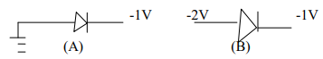
Q3. Select which one is biased forward or reversed?
Q4. How the width of depletion layer varies with increasing forward biasing of pn junction diode?
Q5. Why width and doping concentration of base in a transistor remains to be thin and lightly doped?
Q6. With the help of a diagram explain the term ‘ Deplition layer’ and ‘potential barrier’ in p-n junction diode ?
Q7.W hy a photo diode operated in reverse bias mode? For what purpose is a photodiode used? Draw its I-V characteristics for different intensities of illumination.
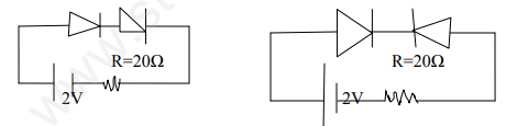
Q8- Determine the current in the resistance R?
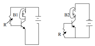
Q9.Write with reason which bulb will glow?Write the effect of increasing resistance R on brightness of the bulb if it glows?
Q10.Which diode is used as a voltage regulator? with the help of circuit diagram explain how we use to this diode as a voltage regulator?
Q11.Identify the logic gate realized by the following circuit? Make its symbol. write its truth table.
Q12.With the help of suitable circuit diagram briefly explain the use of transistor as a switch.
Q13.Draw the transfer characteristic curve of a base biased transistor in CE configuration.Explain clearly how the active region of the V0 vs Vi curve in the transistor is used as an amplifier?And prove that AV=- β rO/ri
Q14.State the principle of a transistor amplifier with positive feedback working as an oscillator.Draw a circuit diagram showing how the feedback can be achieved by induction
coupling to get the self sustained oscillator? Write its working.
Q15.Draw a circuit for drawing the characteristics of transistor. draw the input and output
characteristics. what information we obtain from these graphs?
Q16.(a)In CE transistor amplifier the output signal voltage across collector resistance of 4kohm is
2volt.if the base resistance is 2ohm and the current amplification factor is 100,find the input signal
voltage and current.
(b)explain the working of full wave rectifier.
Important Questions for NCERT Class 12 Physics Semiconductor Devices
Question. In a full wave rectifier circuit operating from 50 Hz mains frequency, what is the fundamental frequency in the ripple?
(a) 50 Hz
(b) 100 Hz
(c) 70 Hz
(d) 25 Hz
Answer : B
Question. Which one of the following is true about the p-type and n-type semi-conductor ?
(a) n-type semi-conductor have holes in majority.
(b) the concentration of electrons and holes are equal in both n-type and p -type semiconductors.
(c) n-type semi-conductors have free electrons in majority.
(d) p-type semi-conductor has excess negative charge.
Answer : C
Question. When added an impurity into the silicon which one of the following produces n-type of semiconductors :
(a) iron
(b) magnesium
(c) aluminium
(d) phosphorous
Answer : D
Question. At 0 K temperature, a p-type semiconductor
(a) has equal number of holes and free electrons
(b) has few holes but no free electrons
(c) has few holes and few free electrons
(d) does not have any charge carriers
Answer : D
Question. The value of current gain a of a transistor is 0.98. The value of b will be
(a) 490
(b) 4.9
(c) 59
(d) 49
Answer : D
Question. To a germanium sample, traces of gallium are added as an impurity. The resultant sample would behave like :
(a) a conductor
(b) a p-type semi-conductor
(c) an n-type sem-iconductor
(d) an insulator
Answer : B
Question. A Ge specimen is doped with Al. The concentration of acceptor atoms is ~1021 atoms/m3. Given that the intrinsic concentration of electron-hole pairs is ~1019/m3, the concentration of electrons in the specimen is
(a) 1017/m3
(b) 1015/m3
(c) 104/m3
(d) 102 /m3
Answer : A
Question. Which of the following logic gates is an universal gate ?
(a) OR
(b) NOT
(c) AND
(d) NAND
Answer : D
Question. Consider an n-p-n transistor amplifier in common emitter configuration. The current gain of the transistor is 100. If the collector current changes by 1mA, what will be the change in emitter current
(a) 1.1 mA
(b) 1.01 mA
(c) 0.01 mA
(d) 10 mA
Answer : B
Question. When a p-n diode is reverse biased, then
(a) no current flows
(b) the depletion region is increased
(c) the depletion region is reduced
(d) the height of the potential barrier is reduced
Answer : B
Question. Zener diode acts as a/an
(a) oscillator
(b) regulator
(c) rectifier
(d) filter
Answer : B
Question. In the half wave rectifier circuit operating from 50 Hz mains frequency, the fundamental frequency in the ripple would be
(a) 25 Hz
(b) 50 Hz
(c) 70.7 Hz
(d) 100 Hz
Answer : B
Question. A transistor is a/an
(a) chip
(b) insulator
(c) semiconductor
(d) metal
Answer : C
Question. If collector current is 120 mA and base current is 2 mA and resistance gain is 3, what is power gain?
(a) 180
(b) 10800
(c) 1.8
(d) 18
Answer : B
Question. Mobilities of electrons and holes in a sample of intrinsic Ge at room temperature are 0.35m2/V–s and 0.18m2/V–s respectively. If the electron and hole densities are each equal to 2.5×10¹⁹/m3, the Ge conductivity will be
(a) 3.12 S/m
(b) 2.12 S/m
(c) 1.12 S/m
(d) 4.12 S/m
Answer : B
Question. An LED (Light Emitting Diode) is constructed from a p–n junction based on a certain Ga–As– P semi–conducting material whose energy gap is 1.9 eV. What is the wavelength of the emitted light?
(a) 650 nm
(b) 65Å
(c) 800 nm
(d) 8000 Å
Answer : A
Question. In n-p-n transistor circuit the collector current is 10 mA. If 90% of the electron reach the collector, then emitter current will be
(a) 1 mA
(b) 0.1 mA
(c) 2 mA
(d) nearly 11 mA
Answer : D
Question. The cause of the potential barrier in a p-n junction diode is
(a) depletion of positive charges near the junction
(b) concentration of positive charges near the junction
(c) depletion of negative charges near the junction
(d) concentration of positive and negative charges near the junction
Answer : D
Question. The expected energy of the electrons at absolute zero is called
(a) Fermi energy
(b) Emission energy
(c) Work function
(d) Potential energy
Answer. A
Question. When a semiconductor is heated, its resistance
(a) Decreases
(b) Increases
(c) Remains unchanged
(d) Nothing is definite
Answer. A
Question. In an insulator, the forbidden energy gap between the valence band and conduction band is of the order of
(a) 1MeV
(b) 0.1MeV
(c) 1eV
(d) 5 eV
Answer. D
Question. The forbidden energy band gap in conductors, semiconductors and insulators are 1 2 EG , EG and 3 EG respectively. The relation among them is
(a) EG1 = EG2 = EG3
(b) EG1 < EG2 < EG3
(c) EG1 > EG2 > EG3
(d) EG1 < EG2 > EG3
Answer. B
Question. Wires P and Q have the same resistance at ordinary (room) temperature. When heated, resistance of P increases and that of Q decreases. We conclude that
(a) P and Q are conductors of different materials
(b) P is N-type semiconductor and Q is P-type semiconductor
(c) P is semiconductor and Q is conductor
(d) P is conductor and Q is semiconductor
Answer. D
Question. In intrinsic semiconductor at room temperature, number of electrons and holes are
(a) Equal
(b) Zero
(c) Unequal
(d) Infinite
Answer. A
Question. If P N and e N be the numbers of holes and conduction electrons in an extrinsic semiconductor, then
(a) P e N > N
(b) P e N = N
(c) P e N < N
(d) P e N > N or P e N < N
depending on the nature of impurity
Answer. D
Question. Fermi level of energy of an intrinsic semiconductor lies
(a) In the middle of forbidden gap
(b) Below the middle of forbidden gap
(c) Above the middle of forbidden gap
(d) Outside the forbidden gap
Answer. A
Question. At room temperature, a P-type semiconductor has
(a) Large number of holes and few electrons
(b) Large number of free electrons and few holes
(c) Equal number of free electrons and holes
(d) No electrons or holes
Answer. A
Question. Which impurity is doped in Si to form N-type semi-conductor?
(a) Al
(b) B
(c) As
(d) None of these
Answer. C
Question. When p-n junction diode is forward biased, then
(a) the depletion region is reduced and barrier height is increased
(b) the depletion region is widened and barrier height is reduced
(c) both the depletion region and barrier height are reduced
(d) both the depletion region and barrier height are increased.
Answer. C
Question. In an unbiased pn junction, electrons diffuse from n-region to p-region because
(a) electrons travel across the junction due to potential difference
(b) electron concentration in n-region is more as compared to that in p-region
(c) only electrons move from n to p region and not the vice-versa
(d) holes in p-region attract them.
Answer. B
Question. In a p-n junction diode, not connected to any circuit
(a) the potential is the same everywhere
(b) the p-type side is at a higher potential than the n-type side
(c) there is an electric field at the junction directed from the n-type side to the p-type side
(d) there is an electric field at the junction directed from the p-type side to the n-type side.
Answer. C
Question. Give the ratio of number of holes and the no. of conduction electrons in an intrinsic semiconductor.
Answer. 𝑛𝑒𝑛ℎ=1 (As in intrinsic semiconductor ne = nh)
Question. A semiconductor has equal electron and hole concentration of 6 x 10⁸ m-3. On doping with a certain impurity electron concentration increases to 3 x 10¹² m-3. Identify the type of semiconductor after doping?
Answer. As ne > nh, thus resulting semiconductor is of n-type.
Question. Why is a semiconductor damaged by a strong current?
Answer. When a strong current passes through a semiconductor large amount of heat is produced which breaks the covalent bonds in the semiconductor due to which it gets damaged.
Question. State the reason, why GaAs is most commonly used in making of a solar cell.
Answer. GaAs is most commonly used in making of a solar cell because :
(i) It has high optical absorption. (ii) It has high electrical conductivity.
Question. In the middle of the depletion layer of reverse biased pn junction, the electric field is …….
Answer. Very small nearly zero
Question. Name the two processes involved in the formation of p-n junction?
Answer. diffusion and drift
Question. Give an approximate value for the potential barrier of silicon type junction diode
Answer. 0.7 v
Question. What is the name of the ability of a junction diode to convert an AC to DC
Answer. Rectification
Question. What do you mean by depletion region and potential barrier in junction diode?
Answer. A layer around the junction between p and n-sections of a junction diode where charge carriers electrons and holes are less in number is called depletion region. The potential difference created across the junction due to the diffusion of charge carriers across the junction is called potential barrier.
Question. What do you mean by hole in a circuit? Write its two characteristics?
Answer. A vacancy created in a covalent bond in a semiconductor due to the release of electron is known as hole in a semiconductor. Characteristics of hole (i) Hole is equivalent to a positive electronic charge. (ii) Mobility of hole is less than that of an electron
Question. What are the advantages and disadvantages of semiconductor devices over vacuum tubes?
Answer. Advantages – Semiconductor devices are very small in size as compared to the vacuum tubes. It requires low voltage for their operation Disadvantage – Due to the rise in temperature and by applying high voltage it can be damage
Question. Why does the width of depletion layer of a p-n junction increase in reverse biasing?
Answer. During reverse biasing, the positive terminal of the external battery attracts electrons from the n-region and its negative terminal attracts holes from the p-region i.e., the majority charge carriers move away from the junction. This increases the width of the depletion layer
Question. Define the terms ‘potential barrier’ and ‘depletion region’ for a p – n junction diode.
State how the thickness of the depletion region will change when the p-n junction diode is (i) forward biased and (ii) reverse biased.
Answer. Potential barrier: The potential barrier is the fictitious battery, which seems to be connected across the p-n junction with its positive terminal in the n-region and the negative terminal in the p-region. Depletion region: The region around the junction, which is devoid of any mobile charge carriers, is called the depletion layer or region. I)When the p-n junction is forward biased, there is a decrease in the depletion region.
Free study material for Physics
CBSE Class 12 Physics Chapter 14 Semiconductor Electronics Materials Devices And Simple Circuits Assignment
Access the latest Chapter 14 Semiconductor Electronics Materials Devices And Simple Circuits assignments designed as per the current CBSE syllabus for Class 12. We have included all question types, including MCQs, short answer questions, and long-form problems relating to Chapter 14 Semiconductor Electronics Materials Devices And Simple Circuits. You can easily download these assignments in PDF format for free. Our expert teachers have carefully looked at previous year exam patterns and have made sure that these questions help you prepare properly for your upcoming school tests.
Benefits of solving Assignments for Chapter 14 Semiconductor Electronics Materials Devices And Simple Circuits
Practicing these Class 12 Physics assignments has many advantages for you:
- Better Exam Scores: Regular practice will help you to understand Chapter 14 Semiconductor Electronics Materials Devices And Simple Circuits properly and you will be able to answer exam questions correctly.
- Latest Exam Pattern: All questions are aligned as per the latest CBSE sample papers and marking schemes.
- Huge Variety of Questions: These Chapter 14 Semiconductor Electronics Materials Devices And Simple Circuits sets include Case Studies, objective questions, and various descriptive problems with answers.
- Time Management: Solving these Chapter 14 Semiconductor Electronics Materials Devices And Simple Circuits test papers daily will improve your speed and accuracy.
How to solve Physics Chapter 14 Semiconductor Electronics Materials Devices And Simple Circuits Assignments effectively?
- Read the Chapter First: Start with the NCERT book for Class 12 Physics before attempting the assignment.
- Self-Assessment: Try solving the Chapter 14 Semiconductor Electronics Materials Devices And Simple Circuits questions by yourself and then check the solutions provided by us.
- Use Supporting Material: Refer to our Revision Notes and Class 12 worksheets if you get stuck on any topic.
- Track Mistakes: Maintain a notebook for tricky concepts and revise them using our online MCQ tests.
Best Practices for Class 12 Physics Preparation
For the best results, solve one assignment for Chapter 14 Semiconductor Electronics Materials Devices And Simple Circuits on daily basis. Using a timer while practicing will further improve your problem-solving skills and prepare you for the actual CBSE exam.
FAQs
You can download free PDF assignments for Class 12 Physics Chapter 14 Semiconductor Electronics Materials Devices And Simple Circuits from StudiesToday.com. These practice sheets have been updated for the 2026-27 session covering all concepts from latest NCERT textbook.
Yes, our teachers have given solutions for all questions in the Class 12 Physics Chapter 14 Semiconductor Electronics Materials Devices And Simple Circuits assignments. This will help you to understand step-by-step methodology to get full marks in school tests and exams.
Yes. These assignments are designed as per the latest CBSE syllabus for 2026. We have included huge variety of question formats such as MCQs, Case-study based questions and important diagram-based problems found in Chapter 14 Semiconductor Electronics Materials Devices And Simple Circuits.
Practicing topicw wise assignments will help Class 12 students understand every sub-topic of Chapter 14 Semiconductor Electronics Materials Devices And Simple Circuits. Daily practice will improve speed, accuracy and answering competency-based questions.
Yes, all printable assignments for Class 12 Physics Chapter 14 Semiconductor Electronics Materials Devices And Simple Circuits are available for free download in mobile-friendly PDF format.