
Download the latest CBSE Class 12 Physics Electronic Devices Notes Set 02 in PDF format. These Class 12 Physics revision notes are carefully designed by expert teachers to align with the 2026-27 syllabus. These notes are great daily learning and last minute exam preparation and they simplify complex topics and highlight important definitions for Class 12 students.
Revision Notes for Class 12 Physics Chapter 14 Semiconductor Electronics Materials Devices and Simple Circuits
To secure a higher rank, students should use these Class 12 Physics Chapter 14 Semiconductor Electronics Materials Devices and Simple Circuits notes for quick learning of important concepts. These exam-oriented summaries focus on difficult topics and high-weightage sections helpful in school tests and final examinations.
Chapter 14 Semiconductor Electronics Materials Devices and Simple Circuits Revision Notes for Class 12 Physics
9. ELECTRONIC DEVICES
GIST
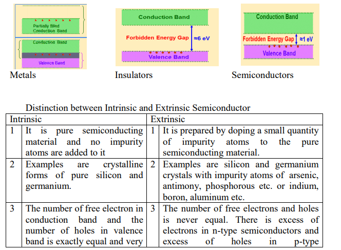
1. In metals, the conduction band and valence band partly overlap each other and there is no forbidden energy gap.
2. In insulators, the conduction band is empty and valence band is completely filled and forbidden gap is quite large = 6 eV. No electron from valence band can cross over to conduction band at room temperature, even if electric field is applied. Hence there is no conductivity of the insulators.
3. In semiconductors, the conduction band is empty and valence band is totally filled. But the forbidden gap between conduction band and valence band is quite small, which is about 1 eV. No electron from valence band can cross over to conduction band. Therefore, the semiconductor behaves as insulator. At room temperature, some electrons in the valence band acquire thermal energy, greater than energy gap of 1 eV and jump over to the conduction band where they are free to move under the influence of even a small electric field. Due

P-n junction diode
Two important processes occur during the formation of p-n junction diffusion and drift. The motion of majority charge carriers give rise to diffusion current.
Due to the space charge on n-side junction and negative space charge region on p-side the electric field is set up and potential barrier develops at the junction electric field e- on p-side moves to n and holes from n-side to p-side which is called drift current.
In equilibrium state, there is no current across p-n junction and potential barrier across p-n junction has maximum value.
The width of the depletion region and magnitude of barrier potential depends on the nature of semiconductor and doping concentration on two sides of p-n junction.
Forward Bias
P-n junction is FB when p-type connected to the +ve of battery and n-type connected to –ve battery Potential barrier is reduced and width of depletion layer decreases.
Reverse Bias
P-n junction in RB p-type connected to the –ve battery and n-type connected to +ve Resistance of p-n junction is high to the flow of current.


Please refer to the link below for CBSE Class 12 Physics Notes - Electronic Devices
Free study material for Physics
CBSE Class 12 Physics Chapter 14 Semiconductor Electronics Materials Devices and Simple Circuits Notes
Students can use these Revision Notes for Chapter 14 Semiconductor Electronics Materials Devices and Simple Circuits to quickly understand all the main concepts. This study material has been prepared as per the latest CBSE syllabus for Class 12. Our teachers always suggest that Class 12 students read these notes regularly as they are focused on the most important topics that usually appear in school tests and final exams.
NCERT Based Chapter 14 Semiconductor Electronics Materials Devices and Simple Circuits Summary
Our expert team has used the official NCERT book for Class 12 Physics to design these notes. These are the notes that definitely you for your current academic year. After reading the chapter summary, you should also refer to our NCERT solutions for Class 12. Always compare your understanding with our teacher prepared answers as they will help you build a very strong base in Physics.
Chapter 14 Semiconductor Electronics Materials Devices and Simple Circuits Complete Revision and Practice
To prepare very well for y our exams, students should also solve the MCQ questions and practice worksheets provided on this page. These extra solved questions will help you to check if you have understood all the concepts of Chapter 14 Semiconductor Electronics Materials Devices and Simple Circuits. All study material on studiestoday.com is free and updated according to the latest Physics exam patterns. Using these revision notes daily will help you feel more confident and get better marks in your exams.
FAQs
You can download the teacher prepared revision notes for CBSE Class 12 Physics Electronic Devices Notes Set 02 from StudiesToday.com. These notes are designed as per 2026-27 academic session to help Class 12 students get the best study material for Physics.
Yes, our CBSE Class 12 Physics Electronic Devices Notes Set 02 include 50% competency-based questions with focus on core logic, keyword definitions, and the practical application of Physics principles which is important for getting more marks in 2026 CBSE exams.
Yes, our CBSE Class 12 Physics Electronic Devices Notes Set 02 provide a detailed, topic wise breakdown of the chapter. Fundamental definitions, complex numerical formulas and all topics of CBSE syllabus in Class 12 is covered.
These notes for Physics are organized into bullet points and easy-to-read charts. By using CBSE Class 12 Physics Electronic Devices Notes Set 02, Class 12 students fast revise formulas, key definitions before the exams.
No, all study resources on StudiesToday, including CBSE Class 12 Physics Electronic Devices Notes Set 02, are available for immediate free download. Class 12 Physics study material is available in PDF and can be downloaded on mobile.