
Practice NEET UG Physics Semiconductor Electronics MCQs provided below. The MCQ Questions for NEET Semiconductor Electronics Physics with answers and follow the latest NEET/ NCERT and KVS patterns. Refer to more Chapter-wise MCQs for NEET NEET Physics and also download more latest study material for all subjects
MCQ for NEET Physics Semiconductor Electronics
NEET Physics students should review the 50 questions and answers to strengthen understanding of core concepts in Semiconductor Electronics
Semiconductor Electronics MCQ Questions NEET Physics with Answers
SUMMARY
Conductor :- · Presence of free electrons
Electrical resistivity is quite less
Insulator :- · No free electrons
· Very large electrical resistivity
Semi-conductor :-
· Electrical resistance greater than conductor but smallar than insulator
· At 0 K temperature it behaves like perfect insulator (in pure form)
Hole :- · An empty space, when covalent bond breaks and electron gets escaped.
· It is electron deficiency space called hole
· behaves like positive electric charge.
For intrinsic (pure) semi-conductor :-
· ni = ne = nh where ni = Intrinsic electrical charge carrier density, ne = number density of electrons nh = number density of holes
· Electrical conduction is due to both, electrons and holes
* Extrinsic semi-conductor :-
(1) N-type : · Pentavalent impurity is added
· Majority charge carrier are electrons
· ne > nh
(2) P-type : · Trivalent imparity is added
· Majority charge carries are holes
· nh > ne
* Valence Band :- Completely filled (with 4N electrons) lower band is called valence band
* Forbidden Gap :- The region above valance band without any available energy levels is called forbidden gap
* Conduction Band :- The region above forbidden gap is called conduction band
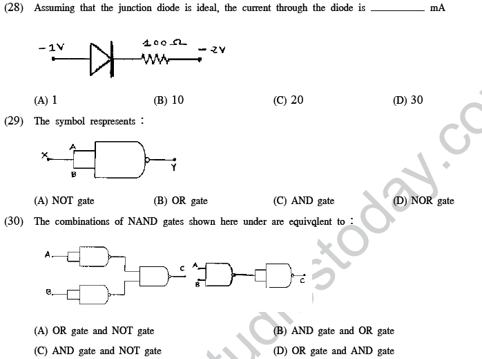
* Band Gap (Eg) :- The difference between minimum energy (Ec) of conduction band and maximum energy
(Ev) of valence band is known as band gap energy
· For Insulator Eg > 3eV
· For Conductor Eg = 0
· For semiconductor Eg < 3eV
* Depletion Region :-
· A region near the junction which is deplete of respective majority charge carriers.
· Thickness is about 0.5mm
* Depletion Barrier :- The varying electrical potential near junction is called depletion barrier (0.7V for Si and 0.3V for Ge)
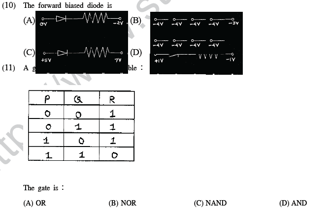
* Forward Bias :-
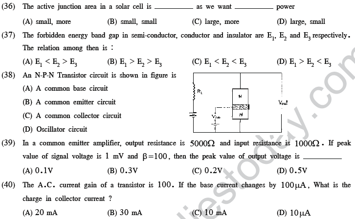
· When P end of PN junction is connected to positive pole of the battery and N end is connected to negative pole of the battery, then such an arrangement is called forward bias.
· Depletion barrier (P.d) and Depletion region (width) is decreased.
* Reverse Bias :-
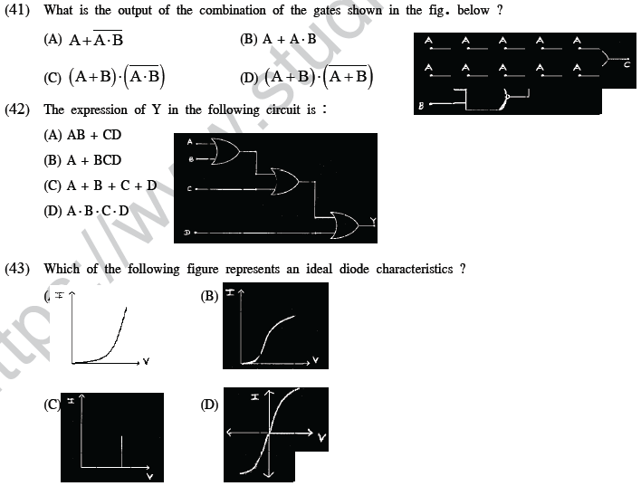
· When P end of PN junction is connected to negative pole of the battery and N end is connected to positive pole of the battery, then such an arrangement is called forward bias.
· Depletion barrier (P.d) and depletion region (width) are increased
* Brekdown voltage :- In reverse bias condition of PN junction, for certain voltage, current increases suddenly. This certain voltage is called breakdown voltage.
* Zener effect :- Due to smaller width of depletion region even at small reverse bias voltage, electric field becomes strong enough to break covalent bond, giving large number of electron hole pair is called zener effect
* Avalanche effect :- Due to large width of depletion region, at only high reverse bias voltage electric field in the depletion region becomes strong enough to break many covalent bonds, giving rise to so many charge carrier is called avalanch effect and diode is called avalanche diode
* Regulated Power Supply :- If D.C. output voltage, in a rectifier circuit (or power supply) remains constant with the charge in load current IL, then such power supply is called regulated power supply
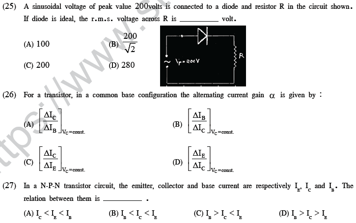
* Rectification and Rectifier :- The process of obtaining D.C. voltage (or current) from A.C. voltage (or current) is called rectification and circuit assembled for this process is called rectifier
* TRANSISTOR
· Transistor is a device made of two PN junctions
· Junction between base and emitter is called emitter junction
· Junction between base and collector is called collector junction
· For proper working of transistor, emitter junction should be forward biased and collector junction should be reverse biased
· A.C. parameters for a transistor
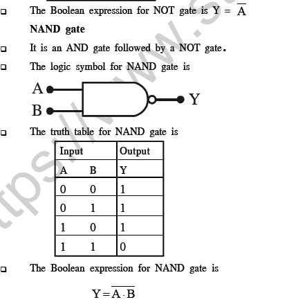
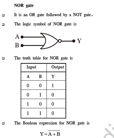
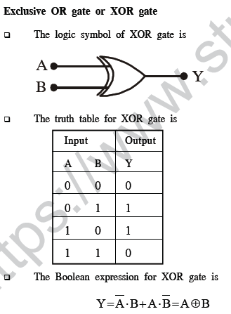
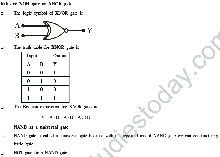
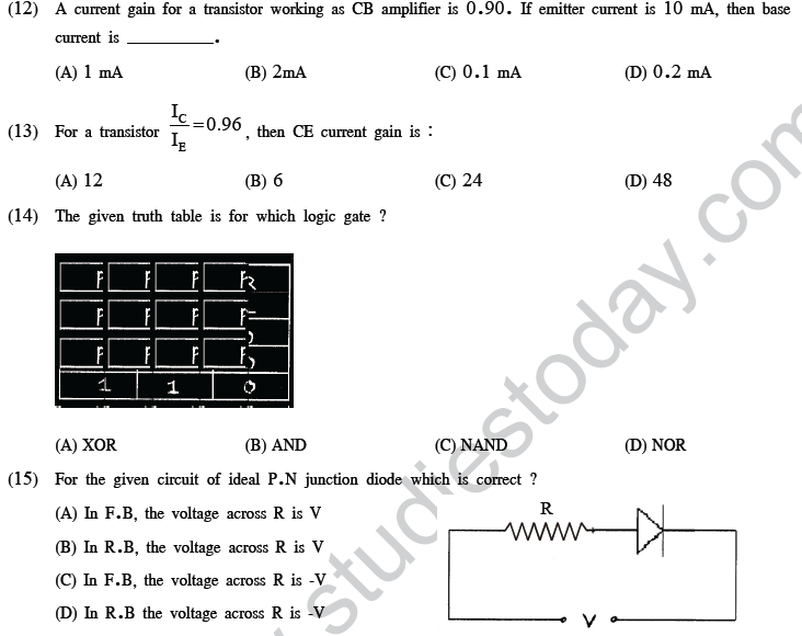
* Logic gate :-
· The logic circuit, with one or more than one input but only one output is called logic gate.
· Basic logic gates are OR gate, AND gate and NOT gate
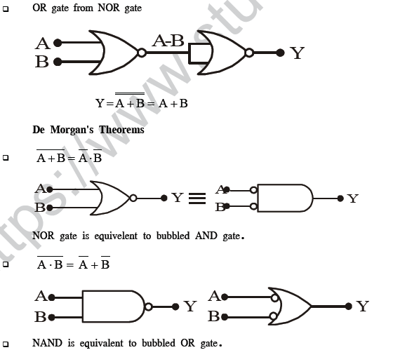
· Universal logic gates are NAND gate and NOR gate
* LOGIC GATES
· A digital circuit with one or more input signals but only one output signal is known as logical gate.
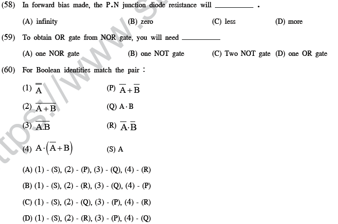
· The logic gates are the building blocks of a digital system. Each logic gate follows a certain logical relationship between input and output voltage.
· There are three basic logic gates :
· OR gate
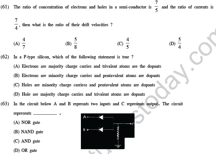
· AND gate
· NOT gate
Truth table
· It is a table that shows all possible input combinations and corresponding output combination for a logic gate.
OR gate
· An OR gate has two or more inputs but only one output.
· It is called OR gate because the output is high if any or all the inputs are high.
· The logic symbol of OR gate is

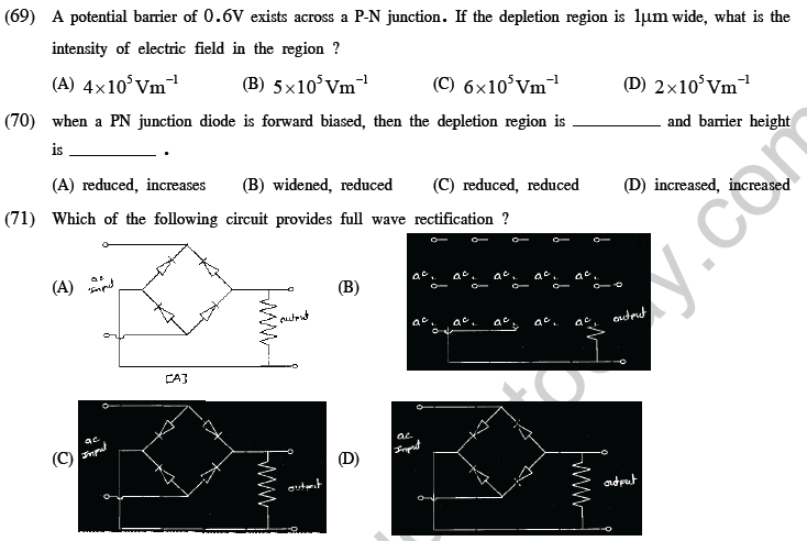
· The Boolean expression for OR gate is
Y = A + B
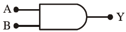
AND gate
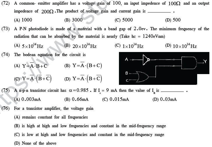
· An AND gate has two or more inputs but only one output.
· It is called AND gate because output is high only when all the inputs are high.
· The logic symbol of AND gate is


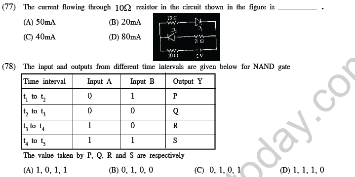
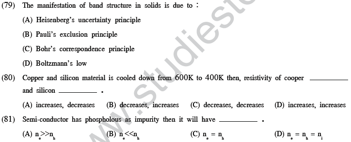
MCQ
For the answer of the following questions choose the correct alternative fromamong the given ones.
(1) C, Si and Ge have same no. of valence electrons. C is an insulator because energy required to take one electron out from
(A) Si is more
(B) C is more
(C) Ge is more
(D) C is less
(2) Ionization energy of isolated phosphorous atonis 10 eV. Ionization energy of same atom in Si is nearlyeV (Relative Permitivity of silicon = 12)
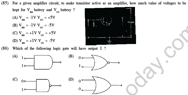
(A) 0.1
(B) 0.2
(C) 0.3
(D) 0.4
(3) By adding impurity in intrinsic semiconductor P type semiconductor is made. charge of these P type semiconductor is
(A) trivalent, neutral
(B) pentaralent, neutral
(C) pentavalent, positive
(D) trivalent, negative
(4) Strong overlaping of different atomic orbitals makes
(A) different energy level
(B) energy band
(C) Conductor
(D) Insulators
(5) We can not make p-n junction diode by making P type semi-condutor join with N - type semi-conductor, because
(A) Inter-atomic spacing becomes less than 1AO
(B) P - type will repel N - type
(C) There will be discontinuity for the flowing charge carriers
(D) semi-conducting properties will be lost
(6) For p-n junction, which statement is incorrect
(A) Donor atoms are depleted of their holes in junction
(B) No net charge exists far from junction
(C) Barrier potential VB is generated
(D) Energy VB is to be surmounted before any charge can flow across junction
(7) The intrinsic semi-conductor has :
(A) a finite resistance which does not change with temperature
(B) infinite resistance which decreases with temperature
(C) Finite resistance which decreases with temperature
(D) Finite resistance which does not change with temperature
(8) The behaviour of Ge as semi-conductor is due to width of :
(A) Conduction band being large
(B) Forbidden band being large
(C) Conduction band being small
(D) Forbidden band being small and narrow
(9) Which of the following is not the advantage of PN junction diode over tube valve ?
(A) Unlimited life
(B) No warming-up time after switching
(C) Large efficiency
(D) Low consumption of Power
16) At 0 K temp, a N - type semi-conductor :
(A) does not have any charge carriers (B) has few holes but no free electrons
(C) few holes and few electrons (D) has equal number of holes and electrons
(17) In Si-crystal, impurity donor atom have valency.
(A) 2 (B) 3 (C) 4 (D) 5
(18) A N-P-N transistor conducts when collector is and emitter is with respect to base.
(A) positive, negative (B) positive, positive
(C) negative, negative (D) negative, positive
(19) A full wave rectifier is operating at 50Hz, 220V the fundamental frequency of ripple will be .
(A) 50 Hz (B) 75 Hz (C) 110 Hz (D) 100 Hz
(20) Reverse bias applied on a junction diode :
(A) raises the potential barrier (B) increases majority charge carrier current
(C) lowers the potential barrier (D) increases the temperature of junction
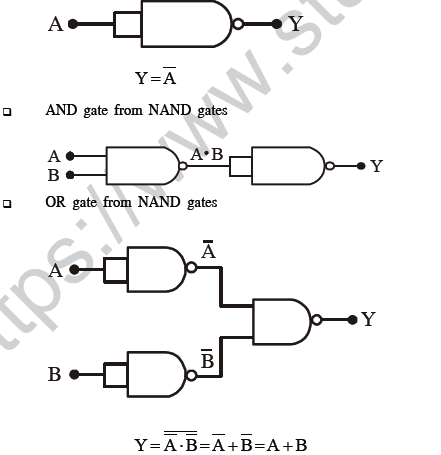
(31) How many NAND gates are used to form AND gate ?
(A) 1 (B) 2 (C) 3 (D) 4
(32) Ripples are .
(A) A.C. mixed with D.C (B) D.C. mixed with output
(C) D.C. output (D) A.C. output
(33) In an P.N.P transistor circuit, the collector current is 10 mA. If 90% of the electrons emitted reach the collector :
(A) IE = 9mA (B) IE = 10mA (C) IB = 1mA (D) IB = -1 mA
(34) When a P-type semi-conductor is heated :
(A) number of holes increases while that of electrons decreases
(B) number of electron increases while that of hole decreases
(C) number of electrons and holes remains same
(D) number of electrons and holes increases equally
(35) The depletion layer in PN junction diode is caused by
(A) drift of holes (B) Diffusion of impurity ions
(C) diffusion of charge carriers (D) drift of electrons
(44) In Ge sample, traces of gallium are added as impurity. The resultant sample would behave like :
(A) a conductor (B) a P-type semiconductor
(C) an N-type semiconductor (D) an insulator
(45) A light emitting diode has a voltage drop of 2V across it when 10mA current is passed. If this LED is to be operated with 6V battery the value of limiting resistor would be .
(A) 400Ω (B) 4000Ω (C) 40kΩ (D) 300Ω
(46) NAND gate is .
(A) A basic gate (B) Not a universal gate
(C) A universal gate (D) Multipurpose gate
(47) The number of holes and electrons in an intrinsic conductors are x and y respectively at room temperature. Which of the following options are true ?
(A) x > y (B) y > x (C) x = y (D) x << y
(48) How will you increase the resistivity of Ge semi-conductor ?
(A) On adding donor impurity (B) On adding acceptor impurity
(C) On making UV light incident on Ge crystal (D) On decreasing the temperature
(49) What is type of material, for the energy band diagram shown in the figure ?
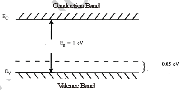
(A) N - type semi-conductor
(B) P - type semi-conductor
(C) Insulator
(D) Intrinsic semi-conductor
(50) From the following semi-conductor devices, operates in forward bias only.
(A) Varactar diode (B) Zener diode (C) Light emitting diode (D) photo-diode
(51) device is the odd-one out.
(A) solar-cell (B) Varactor diode (C) Photodiode (D) Zener diode
(52) The value of depletion capacitance on decreasing the reverse bias on varactor diode
(A) decreases (B) increases (C) becomes zero (D) does not change
(53) Which of the following statement is correct for transistor LC oscillator circuit ?
(A) It works with negative feed back
(B) The phase difference between output and input signal is π radian
(C) To start oscillation external signal is required
(D) The frequency of output signal is independent of the components used in feed back circuit

(64) A zener diode used as voltage regulator is connected _____ .
(i) in forward bias (ii) in reverse bias (iii) in parallel with load (iv) in series with load
(A) (i) and (ii) are correct (B) (ii) and (iii) are correct
(C) only (i) is correct (D) only (iv) is correct
Directions : Question numbers (65), (66) and (67) are based on following passage.
PASSAGE : A n-p-n transistor is used in common emitter made in an amplifier circuit. A change of 40μA in the base current changes the output current by 2mA and 0.04V in input voltage.
(65) The input resistance is .
(A) 1kΩ (B) 10Ω (C) 10 kΩ (D) 100Ω
(66) The current amplification factor is .
(A) 20 (B) 30 (C) 50 (D) 40
(67) If a load of 6kΩ is used, then the voltage gain of the amplifier is .
(A) 100 (B) 200 (C) 300 (D) 400
(68) An amplifier has voltage gain AV = 1000. The voltage gain in dB is .
(A) 20 dB (B) 30 dB (C) 3 dB (D) 60 dB
(82) Zener diode is used as
(A) Full. wave rectifier (B) amplifier
(C) A.C. voltage regulator (D) D.C. voltage regulator
(83) Break down voltage of a diode is 5V. By which effect this breakdown occurs in diode ?
(A) Only avalanche effect (B) Only zener effect
(C) Avalanche or zener effect (D) None of the above
(84) When NPN transistor is used as an amplifier then
(A) electron moves from base to collector
(B) hole travels from emitter to base
(C) hole goes to emitter from base
(D) electron goes to base from collector
(87) For gate, the output is 1 only when both input are `0'
(A) AND (B) NAND (C) OR (D) NOR
(88) In VLSI circuits more than gates are contained.
(A) 1000 (B) 100 (C) 10 (D) 500
(89) The flow of valence electrons to the left means that holes are flowing.
(A) Left (B) Right (C) Either way (D) None
(90) How many free electrons does a P-type semiconductor contain ?
(A) Many (B) None
(C) Only those produced by thermal energy (D) Same number as holes
(91) Suppose an intrinsic semi-conductor at room temperature has 1 billion free electrons at room temperature.
If temperature changes to 75o C, how many holes are there ?
(A) Fewer than 1 billion (B) 1 billion (C) More than 1 billion (D) Impossible to say
(92) Which of the following doesn't fit in the group ?
(A) Conductor (B) Semi conductor (C) Four valence electrons (D) Crystal structure
(93) What kind of device is a diode ?
(A) Bilateral (B) Linear (C) Nonlinear (D) Unipolar
(94) We want a peak load voltage of 40V out of a bridge rectifier, What is the approximate rms value of secondary voltage ?
(A) 0V (B) 14.4V (C) 28.3V (D) 56.6V
(95) The load-current is approximately constant when a zener diode is .
(A) Forward biased (B) Reverse biased
(C) Operating in breakdown region (D) Unbiased
(96) When source voltage increases in a zener diode, which of these current remians approximately constant ?
(A) Series current (B) Zener current (C) Load current (D) Total current
(97) The device associated with voltage controlled capacitance is .
(A) Light emitting diode (B) Photo diode (C) Varactor diode (D) Zener diode
(98) For normal operation of the transistor, the collector diode has to be .
(A) Forward biased (B) Reverse biased
(C) Non conducting (D) Operating in breakdown region
(99) Most of the electrons in the base of N-P-N transistor flow
(A) Out of the base lead (B) Into the collector (C) Into the emitter (D) Into the base supply
Direction for Assertion - Reason type questions
(A) If both Assertion and Reason are true and reason is the correct explanation of assertion.
(B) If both Assertion and Reason are true but Reason is not the correct explanation of assertion.
(C) If Assertion is true but Reason is false
(D) If both assertion and reason are false
(100) A : Intrinsic charge carries are thermally generated
R : Their availability can be easily controlled
(A) (B) (C) (D)
(101) A : Impurity atoms for silicon is selected from third or fourth group
R : These Impurity atoms have same size as that of Si
(A) (B) (C) (D)
(102) A : Photodiode are operated in reverse bias
R : In reverse bias fractional change in minority charge carrier is more
(A) (B) (C) (D)
(103) A : The resistivity of a semi-conductor decreases with temperature
R : At higher temperature more co-valent bond breaks
(A) (B) (C) (D)
(104) A : NAND (or NOR) gates are called digital building blocks
R : The different combination of NAND (or NOR) gates can produce all the basic or complicated gates.
(A) (B) (C) (D)
(105) A : The colour of light emitted by depends on its forward bias.
R : The forward biasing of PN junction diode will increase the width of depletion layer
(A) (B) (C) (D)
(106) A : The ionization energy of isolated phosphorous is very large
R : The ionization energy of phosphorous in lattice is very small
(A) (B) (C) (D)
(107) A : Mostly transistor are used in common emitter configuration
R : Common emitter configuration provide more current gain and small voltage gain
(A) (B) (C) (D)
(108) A : A transistor amplifier circuit in common emitter configuration has low input impednce
R : Base - emitter junction is forward biased
(A) (B) (C) (D)

MCQs for Semiconductor Electronics Physics NEET
Students can use these MCQs for Semiconductor Electronics to quickly test their knowledge of the chapter. These multiple-choice questions have been designed as per the latest syllabus for NEET Physics released by NEET. Our expert teachers suggest that you should practice daily and solving these objective questions of Semiconductor Electronics to understand the important concepts and better marks in your school tests.
Semiconductor Electronics NCERT Based Objective Questions
Our expert teachers have designed these Physics MCQs based on the official NCERT book for NEET. We have identified all questions from the most important topics that are always asked in exams. After solving these, please compare your choices with our provided answers. For better understanding of Semiconductor Electronics, you should also refer to our NCERT solutions for NEET Physics created by our team.
Online Practice and Revision for Semiconductor Electronics Physics
To prepare for your exams you should also take the NEET Physics MCQ Test for this chapter on our website. This will help you improve your speed and accuracy and its also free for you. Regular revision of these Physics topics will make you an expert in all important chapters of your course.
FAQs
You can get most exhaustive NEET UG Physics Semiconductor Electronics MCQs for free on StudiesToday.com. These MCQs for NEET Physics are updated for the 2026-27 academic session as per NEET examination standards.
Yes, our NEET UG Physics Semiconductor Electronics MCQs include the latest type of questions, such as Assertion-Reasoning and Case-based MCQs. 50% of the NEET paper is now competency-based.
By solving our NEET UG Physics Semiconductor Electronics MCQs, NEET students can improve their accuracy and speed which is important as objective questions provide a chance to secure 100% marks in the Physics.
Yes, Physics MCQs for NEET have answer key and brief explanations to help students understand logic behind the correct option as its important for 2026 competency-focused NEET exams.
Yes, you can also access online interactive tests for NEET UG Physics Semiconductor Electronics MCQs on StudiesToday.com as they provide instant answers and score to help you track your progress in Physics.